Quantitative monitoring method and structure for plasma etching

A technology of plasma and etching volume, applied in semiconductor/solid-state device manufacturing, electrical components, circuits, etc., to achieve the effect of simple experimental equipment, strong practicability, and simple monitoring structure

Inactive Publication Date: 2007-10-24
PEKING UNIV
View PDF1 Cites 0 Cited by
  • Summary
  • Abstract
  • Description
  • Claims
  • Application Information

AI Technical Summary

Problems solved by technology

[0004] Gupta from the Massachusetts Institute of Technology (MIT) used the vertical pull-in voltage between the two-end fixed beam and the substrate to judge the etching situation, but the monitoring structure is not sensitive to over-etching.

Method used


Image

  • Quantitative monitoring method and structure for plasma etching
  • Quantitative monitoring method and structure for plasma etching
  • Quantitative monitoring method and structure for plasma etching

Examples


Embodiment

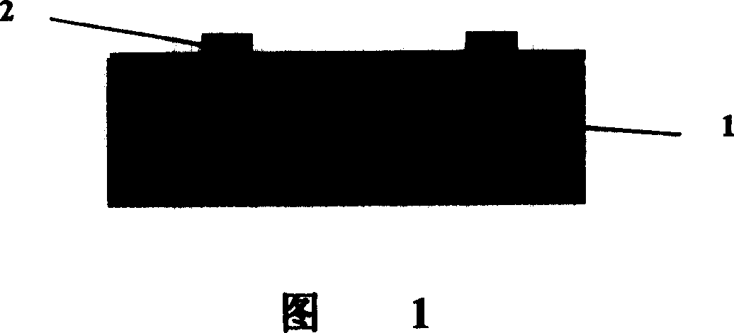
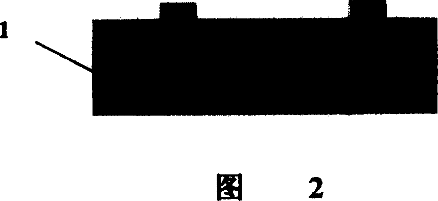
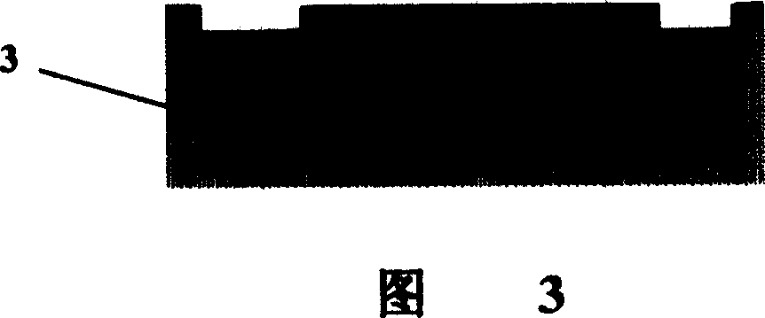
[0068] Next, the cantilever beam monitoring structure with narrow beam and wide spacing is used to quantitatively monitor the ICP etching of different batches of silicon wafers, so that the pull-in voltage of the same monitoring structure that is sensitive to over-cutting on different silicon wafers is close, and two silicon wafers are measured. The pull-in voltage of other identical verification structures is applied to judge whether the over-cutting of these verification structures is close. Since the change of the pull-in voltage is mainly determined by the change of the bending stiffness of the beam and the effective distance between the electrodes, and the change of the bending stiffness of the beam and the effective distance is mainly determined by the overscale, so the change of the pull-in voltage reflects the overscale s difference. When the lateral pull-in voltages of the same etching monitoring structure on different silicon wafers are very close, if the pull-in vol...


PUM

PropertyMeasurementUnit
widthaaaaaaaaaa
lengthaaaaaaaaaa

Abstract

A method for quantitatively monitoring the plasma etching includes such steps as arranging a monitor structure with movable electrode and fixed electrode on the silicon chip to be etched, etching more times, and measuring the lateral attracting voltage between two electrodes to make the lateral attracting voltage close to the lateral attractive voltage relative to the etched quantity to be required. Three structures sensitive to over-etching are also disclosed.

Description

technical field [0001] The invention relates to a monitoring method and structure of a micro-electro-mechanical system (MEMS) processing technology, in particular to a method and a structure for quantitatively monitoring plasma etching in the processing of high aspect ratio microstructures. Background technique [0002] As an interdisciplinary advanced manufacturing technology, MEMS has played an important role in improving people's quality of life, improving people's living standards and enhancing national strength. Among the many MEMS processing technologies, the silicon process is gradually becoming the mainstream process. High aspect ratio silicon etching technology is one of the key processes of silicon MEMS technology. The inductively coupled plasma (ICP) etching system uses high-density plasma for etching, which can produce structures with a thickness of up to hundreds of microns. High aspect ratio MEMS devices (such as accelerometers, gyroscopes, resonators, etc.) a...

Claims


Application Information

Patent Timeline
Patent Type & Authority Patents(China)
IPC IPC(8): C23F1/24H01L21/311
Inventor 贺学锋张大成方竞张钰李婷杨芳王纬
Owner PEKING UNIV
Why Eureka
Try Eureka