

B-ga2o3 single crystal growing method, thin-film single crystal growing method, ga2o3 light-emitting device, and its manufacturing method
A light-emitting device, -ga2o3 technology, applied in the direction of single crystal growth, single crystal growth, crystal growth, etc., can solve problems such as deterioration, hindering the growth of thin film single crystals, and target degradation
- Summary
- Abstract
- Description
- Claims
- Application Information
AI Technical Summary
Problems solved by technology
Method used
Image

Examples
no. 1 approach
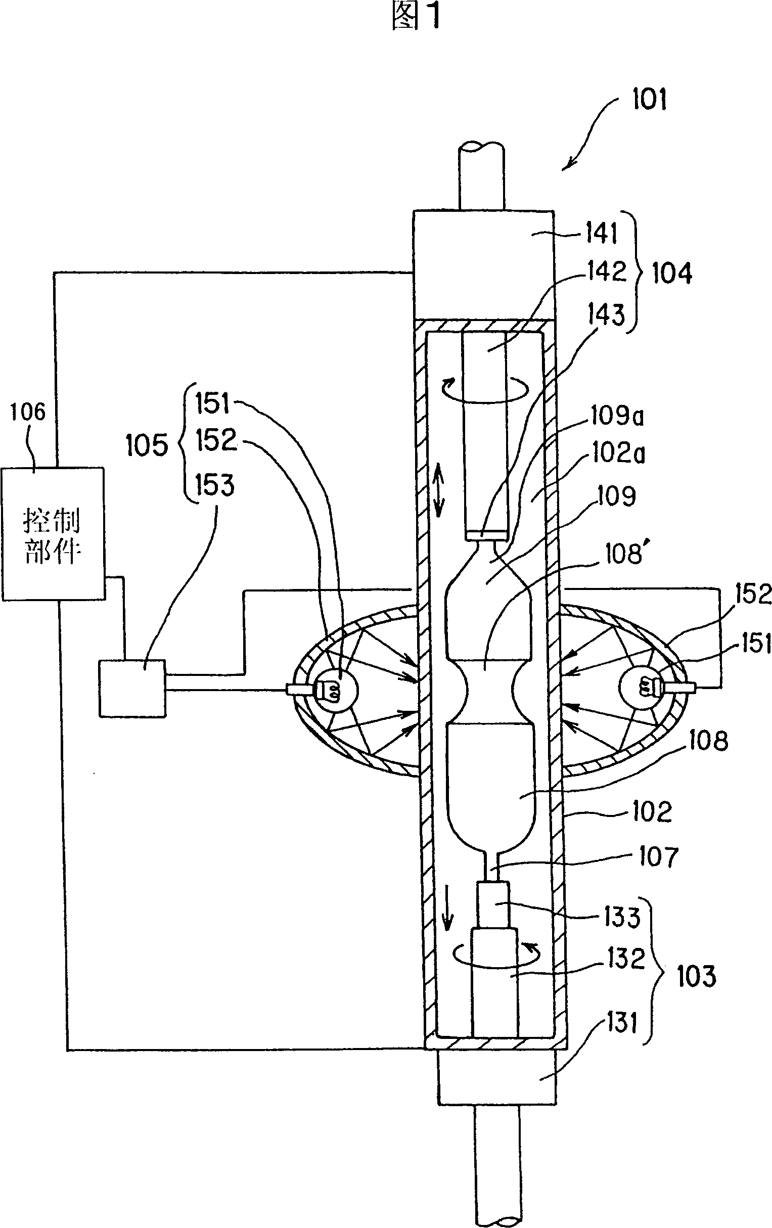
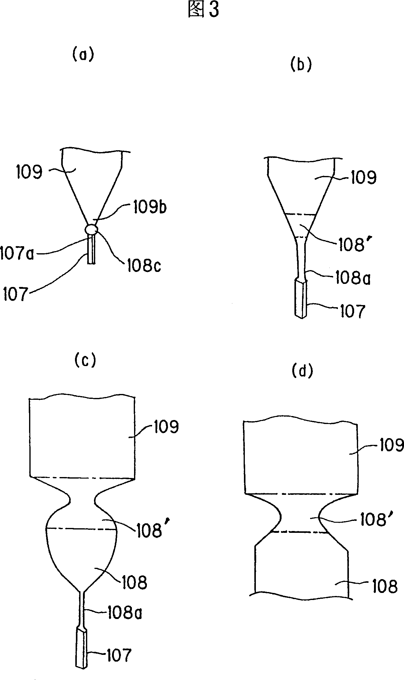
[0053] FIG. 1 shows an infrared heating single crystal manufacturing apparatus according to a first embodiment of the present invention, wherein an infrared heating single crystal manufacturing apparatus 101 is used to manufacture β-Ga according to the FZ method 2 o 3 single crystal, the device schematically consists of a silica tube 102 for clamping / rotating β-Ga 2 o 3 A seed crystal rotating part 103 of a seed crystal (hereinafter referred to as "seed crystal") 107 for clamping / rotating β-Ga 2 o 3 The raw material rotating part 104 of the polycrystalline raw material (hereinafter simply referred to as "polycrystalline raw material") 109, the heating part 105 for heating the polycrystalline raw material 109 to make it melt, the seed crystal rotating part 103 and the control raw material rotating part 104 and the heating part 105 The control unit 106.
[0054] The seed crystal rotating part 103 is provided with a seed chuck that holds the seed crystal 107, a lower rotation...
no. 2 approach
[0083] Fig. 7 shows a schematic configuration of a film forming apparatus according to a second embodiment of the present invention. A film forming apparatus 201 performs film formation according to the PLD method, which is provided with a chamber 202 including a space 220 that can be evacuated, a target table 205 provided in the chamber 202, a target table 203 held on the target table , a rotating mechanical device 211 provided outside the chamber 202 and rotating the target stage 205, a substrate holding member 207 provided inside the chamber 202 and holding the substrate 206, the substrate 206 can be accommodated in the substrate holding member A heater for heating to 1500° C., a radical injecting part 208 for injecting radicals into the chamber 202 through a pipe 202 a, a vacuum pump (not shown) for evacuating the space 220 through a pipe 202 b to evacuate the space 220 and a laser section 204 provided outside the chamber 202 and irradiating a laser beam as an excitation b...
no. 3 approach
[0095] Fig. 8 shows a cross section of a MIS type light emitting device according to a third embodiment of the present invention. The MIS type light emitting device 260 is provided with a β-Ga 2 o 3 Substrate 206 made of single crystal, β-Ga 2 o 3 Thin film single crystal 261, made of β-Ga 2 o 3 Thin film crystals are fabricated and formed on n-type β-Ga 2 o3 The insulating layer 262 on the top of the thin film single crystal 261, the gold electrode 263 formed on the top of the insulating layer 262, the bonding material (bonding) 267 attached to the top of the gold electrode 263 and connected to the lead 268, the n-electrode 264 formed on the bottom of the substrate 206 and Bonding material 265 attached to the bottom of n-electrode 264 and connected to lead 266 .
[0096] By making β-Ga 2 o 3 Crystal annealing forms insulating layer 262 with no oxygen vacancies in the surface of 10-1000 nm.
[0097] According to a third embodiment, a light emitting device with an emis...
PUM
 Abstract
Description
Claims
Application Information