Method for preparing silicon carbide nano-wire with periodical twin crystal structure
A silicon carbide nanowire, periodic technology, applied in the fields of nanostructure manufacturing, nanotechnology, nanotechnology, etc., can solve the problem that the preparation method of silicon carbide nanowires has not been reported.
- Summary
- Abstract
- Description
- Claims
- Application Information
AI Technical Summary
Problems solved by technology
Method used
Image

Examples
Embodiment 1
[0021] 1. Weigh 15 grams of biphenyl and dissolve it in 50 milliliters of acetone, add 0.5 grams of ferric nitrate, and stir to dissolve it.
[0022] 2. Under the condition of constant stirring, add 50 ml of ethyl orthosilicate to the above solution, mix well, add 0.2 g of oxalic acid, and hydrolyze for 24 hours at room temperature to form a sol.
[0023] 3. Add 2 g of hexamethylenetetramine into the sol to form a gel, and dry the resulting gel at 80° C. for 24 hours.
[0024] 4. Put the dry gel into a tube-type high-temperature furnace, pass in argon, heat up to 1200°C, and react at a constant temperature for 10 hours, then naturally cool to room temperature under an argon atmosphere.
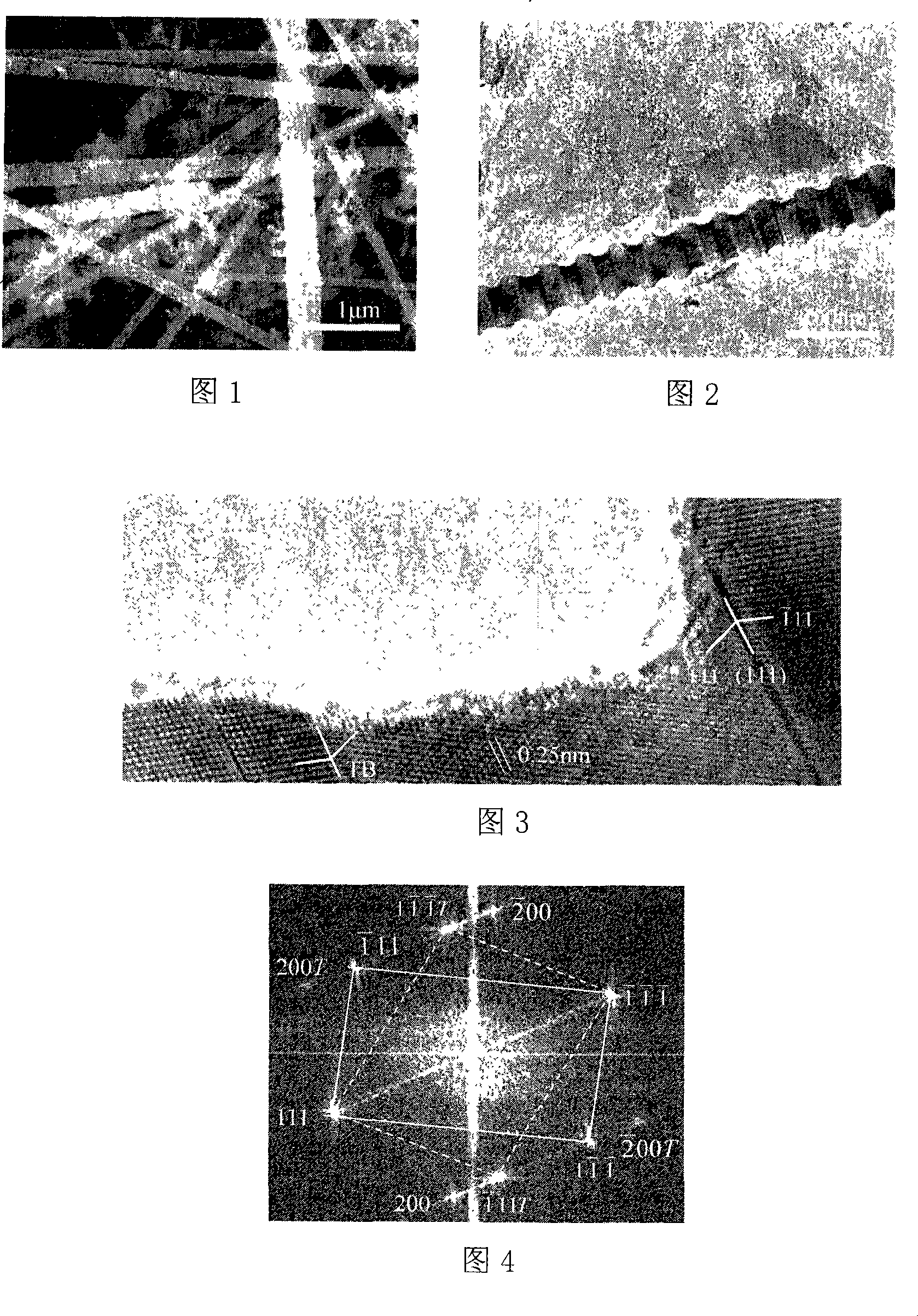
[0025] 5. The obtained reaction product is oxidized in the air at 700°C for 3 hours, then pickled with a mixed acid with a volume ratio of HCl:HF of 1:2, and finally washed with water and dried to obtain the product shown in Figures 1-4. Silicon carbide nanowires with periodic twin structure....
Embodiment 2
[0027] 1. Weigh 20g of biphenyl and dissolve it in 70ml of acetone, add 1g of cobalt nitrate and stir to dissolve it.
[0028] 2. Under the condition of constant stirring, add 70 ml of ethyl orthosilicate to the above solution, mix well, add 0.4 g of oxalic acid, and hydrolyze for 24 hours at room temperature to form a sol.
[0029] 3. 4 grams of hexamethylenetetramine was added to the sol to form a gel, and the obtained gel was dried at 100° C. for 12 hours.
[0030] 4. Put the dry gel into a tube-type high-temperature furnace, pass in argon gas, raise the temperature to 1300°C, and react at constant temperature for 7 hours, then cool it naturally to room temperature under an argon gas atmosphere.
[0031] 5. The obtained reaction product is oxidized in air at 600°C for 4 hours, then pickled with a mixed acid with a volume ratio of HCl:HF of 1:3, and finally washed with water and dried to obtain the product shown in Figures 1-4. Silicon carbide nanowires with periodic twin s...
Embodiment 3
[0033] 1. Weigh 25 grams of biphenyl and dissolve it in 80 milliliters of acetone, add 1 gram of nickel nitrate, and stir to dissolve it.
[0034] 2. Under the condition of constant stirring, add 70 ml of ethyl orthosilicate to the above solution, after mixing evenly, add 0.3 g of oxalic acid, and hydrolyze for 24 hours at room temperature to form a sol.
[0035] 3. Add 3 grams of hexamethylenetetramine into the sol to form a gel, and dry the resulting gel at 110° C. for 24 hours.
[0036] 4. Put the dry gel into a tube-type high-temperature furnace, pass in argon gas, raise the temperature to 1350°C, and react at constant temperature for 6 hours, then cool it naturally to room temperature under an argon gas atmosphere.
[0037] 5. The obtained reaction product is oxidized in the air at 700°C for 5 hours, then pickled with a mixed acid with a volume ratio of HCl:HF of 1:4, and finally washed with water and dried to obtain the product shown in Figures 1-4. Silicon carbide nano...
PUM
 Abstract
Description
Claims
Application Information
 - R&D
- Intellectual Property
- Life Sciences
- Materials
- Tech Scout
- Unparalleled Data Quality
- Higher Quality Content
- 60% Fewer Hallucinations
Browse by: Latest US Patents, China's latest patents, Technical Efficacy Thesaurus, Application Domain, Technology Topic, Popular Technical Reports.
© 2025 PatSnap. All rights reserved.Legal|Privacy policy|Modern Slavery Act Transparency Statement|Sitemap|About US| Contact US: help@patsnap.com