Epoxy resin composition for semiconductor encapsulation and semiconductor device using the same

An epoxy resin and semiconductor technology, applied in semiconductor devices, semiconductor/solid-state device parts, electric solid-state devices, etc., can solve problems such as interface peeling and deformation of flip-chip components

Inactive Publication Date: 2008-06-04
NITTO DENKO CORP
View PDF6 Cites 2 Cited by
  • Summary
  • Abstract
  • Description
  • Claims
  • Application Information

AI Technical Summary

Problems solved by technology

[0011] In addition, when the flip-chip module is sealed with resin by transfer molding using the above-mentioned sealing material, the following problems arise: (1) an unfilled portion is formed in the gap between the semiconductor element and the substrate, thereby creating a void; (2) ) In the moisture resistance reliability evaluation after molding, there will be interface peeling between the semiconductor element and the sealing resin and the interface peeling with the solder resist portion on the substrate; (3) Deformation of the flip chip module

Method used


Image

  • Epoxy resin composition for semiconductor encapsulation and semiconductor device using the same
  • Epoxy resin composition for semiconductor encapsulation and semiconductor device using the same
  • Epoxy resin composition for semiconductor encapsulation and semiconductor device using the same

Examples


Embodiment 1~6、 comparative example 1~9

[0131] The components shown in the following Tables 1 to 3 were blended according to the ratios shown in the tables, and melted and kneaded for 3 minutes in a twin-roll kneader (temperature 100° C.). Next, after the molten material is cooled, it is pulverized to obtain a desired epoxy resin composition for encapsulating a semiconductor. And, "part" means a weight part.

[0132] [Table 1] (parts)

[0133]

[0134] [Table 2] (parts)

[0135]

[0136] [Table 3] (parts)

[0137]

[0138] Using the epoxy resin compositions obtained in these Examples and Comparative Examples, the embedding void resistance and deformation were measured by the following methods, and the pressure cooker retort test (PCT test) was evaluated. The obtained results are collectively shown in Tables 4 to 6 below.

[0139] [Embedding void resistance]

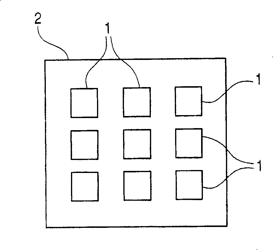
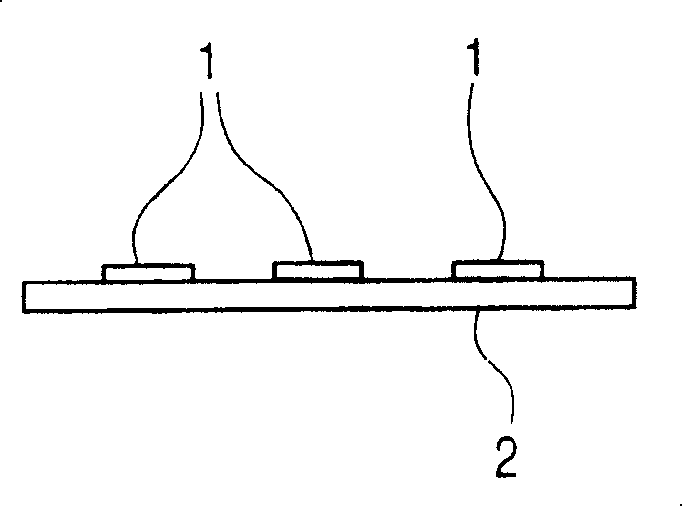
[0140] like Figure 1A and Figure 1B As shown, it is manufactured by mounting nine semiconductor elements 1 (chip size: 10 mm x 10 mm x thickne...

Embodiment 17~32、 comparative example 10~23

[0156] The components shown in the following Tables 7 to 10 were blended according to the ratios shown in the tables, and melt-kneaded for 3 minutes in a twin-roll kneader (at a temperature of 100° C.). Next, after cooling this molten material, it pulverizes, and obtains the desired epoxy resin composition for semiconductor sealing. And, "part" means a weight part.

[0157] [Table 7] (parts)

[0158]

[0159] [Table 8] (parts)

[0160]

[0161] [Table 9] (parts)

[0162]

[0163] [Table 10] (parts)

[0164]

[0165] Using the epoxy resin compositions obtained in these Examples and Comparative Examples, occurrence and deformation of unfilled were measured by the following method, and pressure cooker retort test (PCT test) was evaluated. The obtained results are collectively shown in Tables 11 to 14 below.

[0166] [Fillability and Occurrence of Interfacial Peeling]

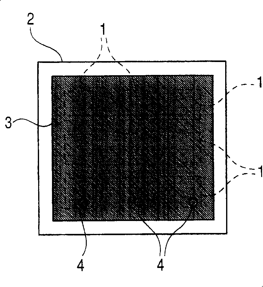
[0167] like Figure 3A and Figure 3B As shown, nine semiconductor elements 5 (chip size: 7mm×...


PUM

PropertyMeasurementUnit
particle diameteraaaaaaaaaa
particle sizeaaaaaaaaaa

Abstract

PROBLEM TO BE SOLVED: To provide an epoxy resin composition for sealing a semiconductor excellent in fillability and void resistance, for example, in a flip chip package and capable of suppressing generation of warpage.

Description

field of invention [0001] The present invention relates to an epoxy resin composition for semiconductor sealing which is excellent in moldability and moisture resistance reliability in single-sided sealing type packages generally called ball grid array (BGA) packages and in packages called flip chip package types And a semiconductor device using the composition. Background technique [0002] From the standpoint of protecting the external environment and that semiconductor elements can be attached and detached, semiconductor elements such as transistors, ICs, and LSIs are sealed by plastic packaging or the like to form semiconductor devices. Recently, along with the demand for thinner semiconductor devices and high-density packaging, there is a strong need to thin single-sided sealed packages such as BGA packages and to package and stack semiconductor elements in a stacked state. [0003] As a sealing material excellent in fluidity and the like for such a BGA package, for ex...

Claims


Application Information

Patent Timeline
Patent Type & Authority Patents(China)
IPC IPC(8): C08G59/00C08L63/00C08G59/62C08K9/06H01L23/29H01L23/31
CPCH01L24/97H01L2224/16225H01L2924/181H01L2924/00012
Inventor 秋月伸也丰田庆池村和弘石坂刚西冈务
Owner NITTO DENKO CORP
Why Eureka
Try Eureka