
Structure of LED, and fabricating method

A technology of light-emitting diodes and manufacturing methods, which is applied in the direction of electrical components, circuits, semiconductor devices, etc., can solve the problems of affecting the pass rate of processing technology, the efficiency of light-emitting diodes, and the fragility of light-emitting diodes, so as to facilitate heat dissipation, increase brightness, low loss effect

Active Publication Date: 2008-06-11
OPTO TECH
View PDF6 Cites 0 Cited by
  • Summary
  • Abstract
  • Description
  • Claims
  • Application Information

AI Technical Summary

Problems solved by technology

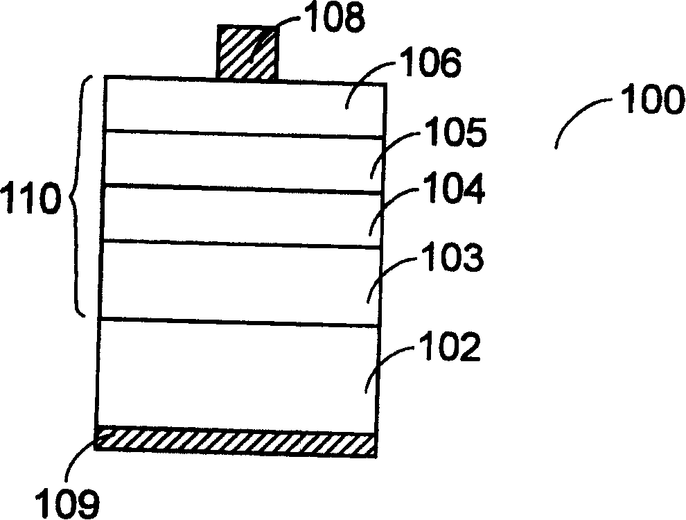
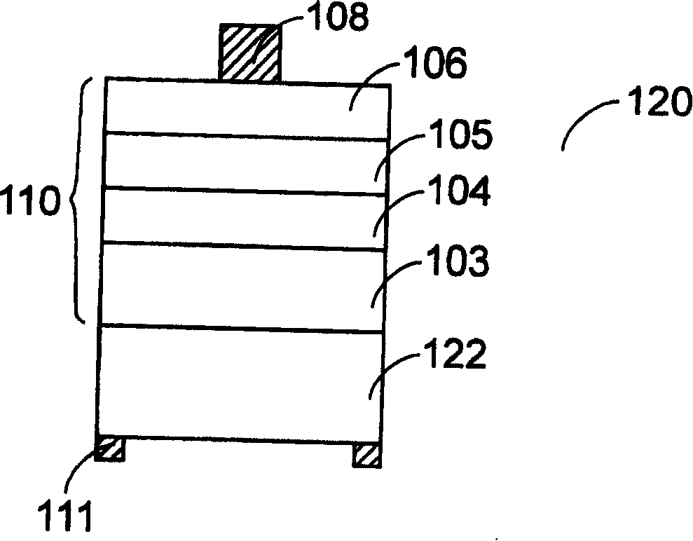
[0013] Similarly, before the temporary substrate 102 and the permanent substrate joint 122 are removed in the processing technology of the above-mentioned light emitting diode, the mechanical strength of the light-emitting region 110 is easily broken during the processing process due to the lack of the support of the temporary substrate 102, which also affects the quality of the processing technology. Pass rate
Furthermore, because the first and second electrodes are produced after the chip bonding step is completed, the process must go through the step of temperature fusion (Alloy), which makes the efficiency of the light emitting diode worse.

Method used


Image

  • Structure of LED, and fabricating method
  • Structure of LED, and fabricating method
  • Structure of LED, and fabricating method

Examples


Embodiment Construction

[0080] In view of the above shortcomings, the present invention proposes a chip bonding light emitting diode to solve the shortcomings of known light emitting diodes manufactured by chip bonding technology. Please refer to Figure 9 , which is a schematic diagram of the structure of the grain-bonded light-emitting diode of the present invention. The structure of the die-bonded light-emitting diode 500 includes a first electrode 508, a light-emitting region 510, an ohmic contact point (Ohmic Contact Dot) 520, a reflective layer 522, a barrier layer (Barrier Layer) 524, an adhesive layer (Eutectic Layer) 526, a visual It is the metal layer (Metal Layer) 528 of the second electrode, and the sub-adhesive substrate (Submount) 530 . Among them, the first electrode 508, the light emitting region 510, the Ohmic Contact Dot (Ohmic Contact Dot) 520, the reflective layer 522, the barrier layer (Barrier Layer) 524, and the paste layer 526 are regarded as a chip (Chip) 550, and the first ...


PUM

PropertyMeasurementUnit
porosityaaaaaaaaaa

Abstract

The structure of LED includes following parts: permanent baseplate possessing first surface; being located on the first surface, the metal layer is divided to first region and second region, and the first region is as first electrode; crystal grain is located at second region of the metal layer. The crystal grain includes at least stacked second electrode and luminous region. Through junction technique of crystal grain, the crystal grain is jointed to the second region of the metal layer so as to form electrical connection between metal layer and luminous region. Overcoming issue of light absorbed by base plate, the invention raises luminous efficiency greatly. Processing technique in low temperature for fusing chip and base plate does not deteriorate chip. Features are: high qualification rate of products, easy of heat elimination. The disclosed structure is suitable to application of LED in high power.

Description

technical field [0001] The present invention relates to a structure of a light emitting diode and a manufacturing method thereof, and in particular to a structure of a chip bonding light emitting diode and a manufacturing method thereof. Background technique [0002] Please refer to figure 1 , which is a schematic diagram of a known aluminum indium gallium phosphide quaternary light emitting diode (AlGaInP Quaternary Light Emitting Diode). The structure of the quaternary light emitting diode 100 grows a light emitting region (Light Emitting Region) 110 on an n-type doped GaAs (n-doped GaAs) substrate (Substrate) 102 . The light emitting region 110 includes an n-doped aluminum indium gallium phosphide (n-doped AlGaInP) layer 103 grown on an n-doped gallium arsenide substrate (n-doped GaAs) 102, grown on an n-doped phosphide Aluminum indium gallium phosphide active layer (AlGaInP Active layer) 104 on aluminum indium gallium (n-doped AlGaInP) layer 103, p-type doped aluminum ...

Claims


Application Information

Patent Timeline
Patent Type & Authority Patents(China)
IPC IPC(8): H01L33/00
Inventor 蔡长达马景时
Owner OPTO TECH
Learn More