A flip-chip LED chip and its manufacturing method

A LED chip and flip-chip technology, which is applied in the direction of electrical components, circuits, semiconductor devices, etc., can solve the problems of poor current diffusion effect of P-type GaN layer, increase of chip turn-on voltage, and decrease of light efficiency of flip-chip, etc. Achieve low resistance ohmic contact, prevent light leakage, and reliable performance

Active Publication Date: 2018-04-13
宁波奕丰光电科技有限公司
View PDF4 Cites 0 Cited by
  • Summary
  • Abstract
  • Description
  • Claims
  • Application Information

AI Technical Summary

Problems solved by technology

However, at high temperature, metal silver is prone to pilling and aggregation, which leads to a decrease in reflectivity, and the light efficiency of flip chips is greatly reduced.
Although alloyed at a lower temperature (such as 200-400°C), the reflectivity of silver can be maintained at about 90%, but the contact resistance between it and the P-type gallium nitride layer will increase, resulting in an increase in the turn-on voltage of the chip
Therefore, high reflectivity and low contact resistance form a pair of contradictions that are difficult for metal alloys.
In addition, in order to reduce the interlayer stress of the GaN-based flip-chip LED chip with this structure, it is necessary to make the first barrier layer and the second barrier layer, which not only leads to a more complicated process, but also because the thermal expansion coefficients of each layer of metal are different. , during subsequent packaging and use, thermal stress may lead to poor adhesion between part of the silver and the P-type GaN layer, resulting in poor current diffusion effect of the P-type GaN layer and uneven light emission of the chip

Method used


Image

  • A flip-chip LED chip and its manufacturing method
  • A flip-chip LED chip and its manufacturing method
  • A flip-chip LED chip and its manufacturing method

Examples


Embodiment Construction

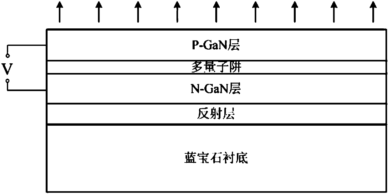
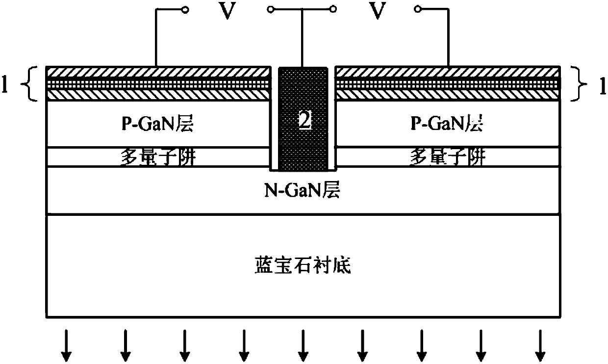
[0041] Such as image 3 , 4 As shown, in a preferred embodiment of the present invention, a flip-chip LED chip is provided. The flip-chip LED chip includes a sapphire substrate and an N-type gallium nitride layer, a multi-quantum well structure layer and a P-type gallium nitride layer distributed upwards from the upper surface of the sapphire substrate, which is a mirror symmetrical structure. The N-type gallium nitride layer, the multi-quantum well structure layer and the P-type gallium nitride layer constitute an epitaxial structure, and the epitaxial structure is perpendicular to the longitudinal section of the symmetry plane of the flip-chip LED chip (in this application, gallium nitride-based flip-chip LED The longitudinal section of the chip and the epitaxial structure refers to the section perpendicular to the symmetry plane) into a convex shape.

[0042] The flip-chip LED chip of this structure can form N-type gallium nitride layer, multi-quantum well structure layer...


PUM


Abstract

The invention discloses an inverted LED (light emitting diode) chip. The inverted LED chip is of a structure of mirror symmetry, wherein an N-type gallium nitride layer, a multi-quantum well structural layer and a P-type gallium nitride layer are sequentially distributed upwards on the upper surface of a sapphire substrate to form an epitaxial structure with a raised longitudinal cross section; a first part and a second part, exposed outside the multi-quantum well structural layer, of the upper surface of the N-type gallium nitride layer respectively form two shoulders of the epitaxial structure, an elongated first N electrode and an elongated second N electrode are respectively distributed on the first part and the second part and extend along the direction parallel to a symmetric surface of the inverted LED chip; and a metal layer NiAgNi with the thickness of a first metal layer Ni being 3-30 angstrom is arranged on the upper surface of the P-type gallium nitride layer, is used as a reflection conducting layer and is also used as a P electrode. The invention also discloses a manufacturing method of the inverted LED chip. The inverted LED chip has the advantages of high optical efficiency, simple production flow and high reliability; and moreover, the inverted LED chip is simple in flow and high in reliability.

Description

technical field [0001] The invention relates to the technical field of LED chips, in particular to a flip-chip LED chip and a manufacturing method thereof. Background technique [0002] With the rise of the third-generation semiconductor materials represented by GaN, blue light and white light-emitting diodes (LEDs) coated with blue phosphors have been successfully developed, and LEDs have become new solid-state light sources in the field of general lighting. Due to its high reliability, energy saving, environmental protection and other advantages, with the continuous improvement of luminous efficiency, the continuous upgrading of LED applications and the market demand for LEDs, LEDs are developing in the direction of high power and high brightness. [0003] The basic structure of a gallium nitride-based LED chip includes a sapphire substrate, an N-type gallium nitride (N-GaN) layer, a multi-quantum well structure layer (light-emitting layer) and a P-type gallium nitride (P-...

Claims


Application Information

Patent Timeline
Patent Type & Authority Patents(China)
IPC IPC(8): H01L33/20H01L33/40H01L33/38H01L33/46
CPCH01L33/20H01L33/385H01L33/405H01L33/46H01L2933/0016
Inventor 田洪涛陈祖辉
Owner 宁波奕丰光电科技有限公司
Why Eureka
Try Eureka