Lighting stick with LBD wafer

A technology of light-emitting diodes and light-emitting sticks, applied in the field of light-emitting sticks, can solve the problems of adverse effects of light-emitting sticks, small heat dissipation area, and poor heat dissipation effect, and achieve the effects of facilitating large-scale production, increasing heat dissipation area, and increasing production speed

Inactive Publication Date: 2008-10-01
黄虎钧
View PDF9 Cites 0 Cited by
  • Summary
  • Abstract
  • Description
  • Claims
  • Application Information

AI Technical Summary

Problems solved by technology

[0004] 1. The heat dissipation area is small: the heat is dissipated by a piece of aluminum substrate under the circuit board, and the heat of the light-emitting diode is mainly generated by its negative terminal. The heat must first pass through the circuit board to be transmitted to the aluminum substrate, and the circuit board itself will block the flow of heat. Conduction, poor cooling effect
[0005] 2. Poor light concentrating effect: each light emitting diode can be regarded as a point light source, and the light emitted by it includes side light and scattered light, which cannot be converged, which reduces the brightness of the light stick, and must be compensated by increasing the number of light emitting diodes Lack of brightness
[0006] 3. Short length: relying only on the support of the sheet-shaped aluminum substrate, the structural strength is poor, and it is easy to bend and deform. The light-emitting stick cannot be made very long, and it is difficult to industrialize large-scale production
[0007] 4. The positive and negative terminal welding wires of the light-emitting diode chip are connected to the pins at both ends of the housing. The positive and negative terminal welding wires are very thin gold wires with low thermal impedance, and the pins play the role of supporting the housing. It is a relatively thick aluminum strip, the pins are welded on the circuit board with tin, the solder joints are very large, the thermal impedance of the junction between the pins and the solder joints is high, and it is easy to generate heat, which will have an adverse effect on the light stick
[0008] Exactly because of the above reasons, the existing luminous sticks are not generally adopted, and the market share is less than 10%.

Method used


Image

  • Lighting stick with LBD wafer
  • Lighting stick with LBD wafer
  • Lighting stick with LBD wafer

Examples


Embodiment Construction

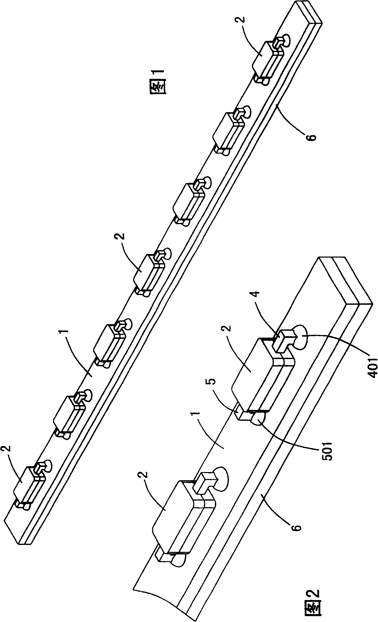
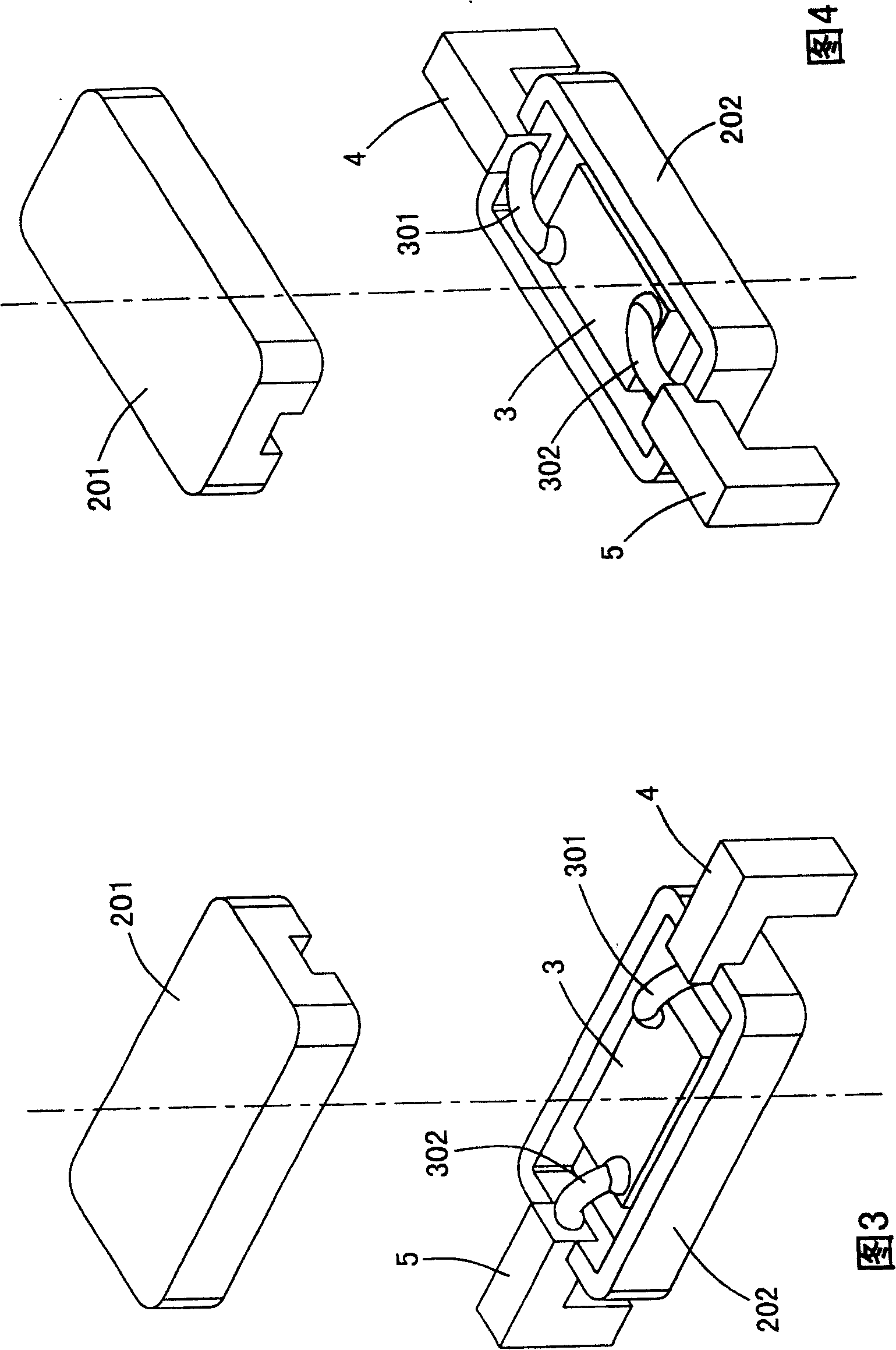
[0037] Label in the figure

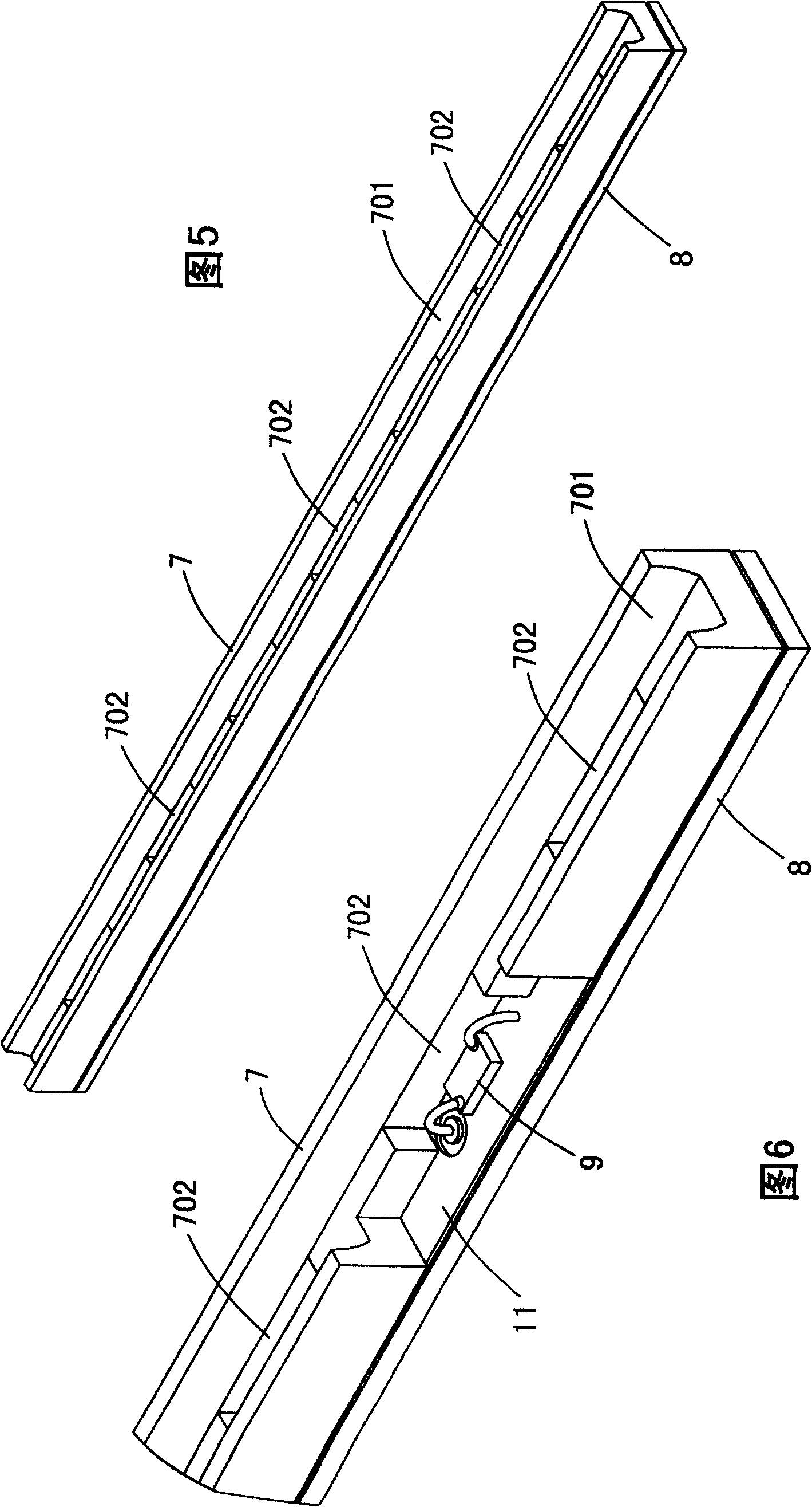
[0038] 1. Circuit board 2. Light-emitting diode 201. Top cover 202. Base 3. Light-emitting diode chip 301. Negative terminal soldering wire 302. Positive terminal soldering wire 4. Pin 401. Tin solder joint 5. Pin 501. Tin solder joint 6. Aluminum substrate 7. Frame 701. Groove 702. Vertical hole 8. Circuit board 9. Light-emitting diode chip 901. Negative terminal welding wire 902. Positive terminal welding wire 11. Negative electrode welding plate 111. Through hole 12. Positive electrode welding Plate 13. Transparent Silicone

[0039] In order to facilitate a better understanding of the essential features of the present invention, firstly introduce the structure of the existing light stick. Please refer to Fig. 1, Fig. 2, Fig. 3, Fig. 4, the structure of the existing luminous stick is: a plurality of light-emitting diodes 2 are arranged at intervals on the strip-shaped circuit board 1, and each light-emitting diode 2 is composed of a housing and ...


PUM


Abstract

A light emitting stick having LED chips (9) is disclosed. The light emitting stick comprises a strip shaped frame (7), a circuit board (8) and a plurality of LED chips (9). The upper part of the frame has a groove (701), and the lower part of the frame has a plurilty of vertical holes (702). The top of each of the vertical holes (702) and the bottom of the groove (701) are feedthrough. A negative pole plate (11) is placed on the upper surface of the circuit board (8), and has a plurality of throughholes (111). The position of the throughholes (111) corresponds to the position of the vertical holes (702). The circuit board (8) has a pluralityof positive pole pads (12). The positive pole pads (12) are exposed from the throughholes (111) on the negative pole plate (11), respectively. The bottom surface of the frame (7) bonds to the negative pole plate (11). The LED chips (9) are embedded into the vertical holes (702) of the frame (7), respectively. The positive terminal wires (902) of the LED chips (9) are connected to the positive terminal wires (902) of the positive pole pad (12) one by one, and the negative terminal wires (901)of the LED chips (9) are connected to the negative pole plate (11) of the circuit board (8) one by one. The inner walls of the groove (701) form reflective walls.

Description

technical field [0001] The invention belongs to the field of optoelectronic technology, and relates to a luminous rod, in particular to a luminous rod composed of light-emitting diodes. The luminous rod can be used as a liquid crystal backlight source or a projection light source, and can also be used for illumination. Background technique [0002] Commonly used backlights for computers and TV LCD screens include cold cathode fluorescent lamps, electroluminescence, and light sticks. [0003] The structure of the existing luminous rod is: a plurality of light-emitting diodes are arranged at intervals on a strip-shaped circuit board, each light-emitting diode is composed of a housing and a light-emitting diode chip packaged in the housing, and the positive and negative sides of the light-emitting diode chip The terminal welding wires are connected with the pins at both ends of the shell, and the pins are soldered on the circuit board with tin, and there is an aluminum substrat...

Claims


Application Information

Patent Timeline
Patent Type & Authority Patents(China)
IPC IPC(8): H01L25/00H01L25/075F21L2/00F21S4/00F21V23/00F21K99/00
CPCF21S4/003F21K9/00F21Y2101/02F21V31/04F21S4/20F21Y2115/10H01L24/97H01L2224/45144H01L2224/48091H01L2224/73265H01L2924/00014H01L2924/00
Inventor 黄虎钧
Owner 黄虎钧
Why Eureka
Try Eureka