

Automatic material transport system for semiconductor production
A transportation system and semiconductor technology, applied in the direction of transportation and packaging, conveyor objects, furnaces, etc., can solve the problems of bulky, space-occupied and inconvenient to use, and achieve the effect of easy movement, three-dimensional space saving, and convenient movement
- Summary
- Abstract
- Description
- Claims
- Application Information
AI Technical Summary
Problems solved by technology
Method used
Image

Examples
Embodiment Construction
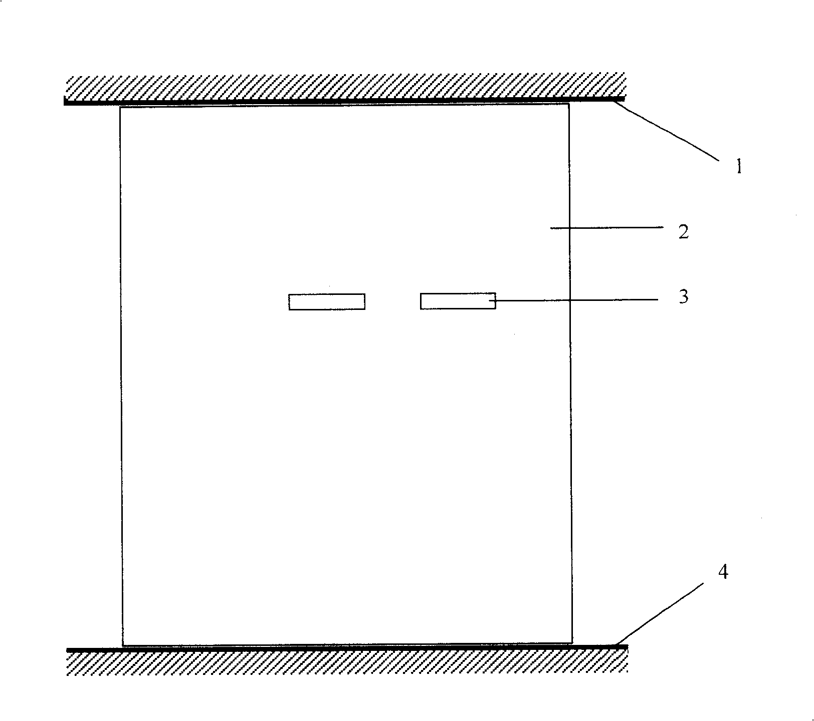
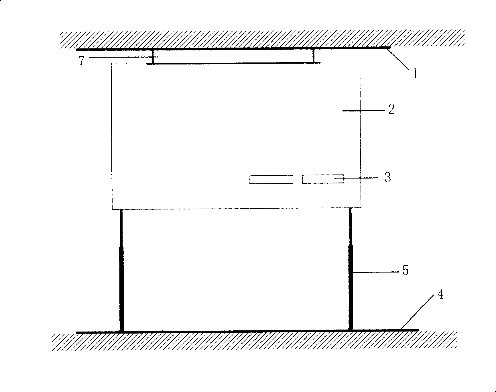
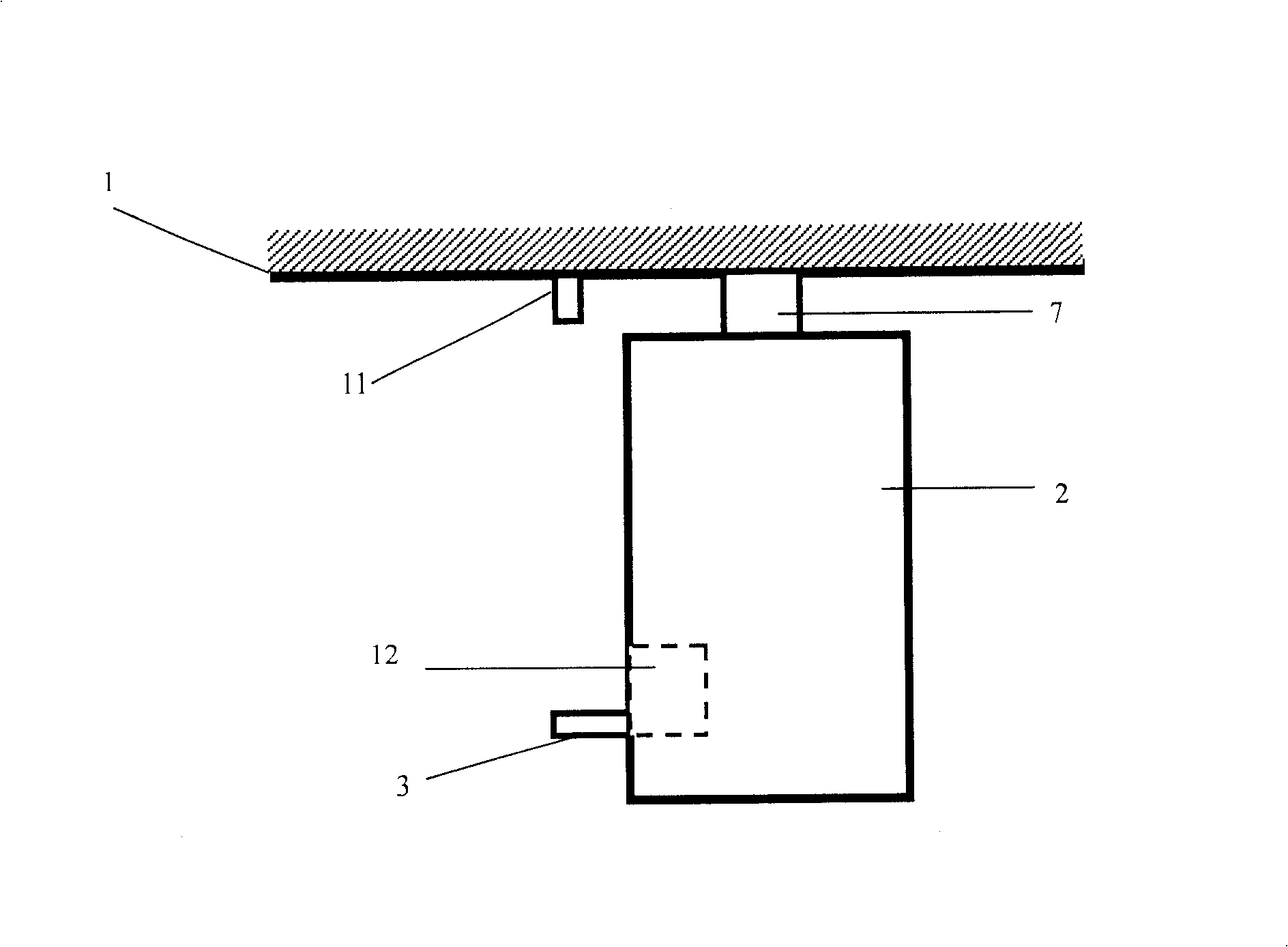
[0034] The invention discloses an automatic material transportation system for semiconductor manufacturing, which can greatly save the three-dimensional space in the FAB. The automatic material transportation system disclosed by the present invention realizes loading and unloading of the materials in the storage boxes in the WIP storage unit of the vertical conveyor belt by using an aerial elevator located above each storage box.
[0035] The automated material handling system of the present invention can be applied in a product manufacturing environment, such as a clean environment for manufacturing IC chips, to automatically store and transport WIP components between workstations and / or processing machines. Includes WIP storage unit and aerial lift delivery subsystem. The storage box includes a plurality of input and output windows in which the cassette container FOUP is placed. The aerial elevator conveying subsystem includes a suspended rail and a plurality of aerial elev...
PUM
 Abstract
Description
Claims
Application Information