Heat radiation type packaging structure and its making method

A packaging structure and heat dissipation technology, which is applied in semiconductor/solid-state device manufacturing, electrical components, electrical solid-state devices, etc., can solve the problems of large stamping or cutting tool loss, inability to greatly improve production efficiency, and affect the appearance of packages, etc. Less wear and tear, conducive to cutting cost control, not easy to produce burrs

Inactive Publication Date: 2008-12-24
SILICONWARE PRECISION IND CO LTD
View PDF5 Cites 0 Cited by
  • Summary
  • Abstract
  • Description
  • Claims
  • Application Information

AI Technical Summary

Problems solved by technology

[0012] However, in the above-mentioned semiconductor package process, when the singulation step is performed, because the singulation tool directly passes through the heat sink, and because the heat sink is generally made of a metal material with a hard texture and sufficient thickness, no matter whether it is used during singulation When punching or cutting with a diamond knife, the peripheral material of the heat sink will produce uneven sharp-edged edges (or burrs) due to pulling, which will affect the appearance of the package, and will also cause excessive loss of punching or cutting tools , resulting in a substantial increase in cost, and the production efficiency cannot be greatly improved

Method used


Image

  • Heat radiation type packaging structure and its making method
  • Heat radiation type packaging structure and its making method
  • Heat radiation type packaging structure and its making method

Examples


Embodiment 1

[0043] See Figure 4A to Figure 4F , It is a schematic diagram of the manufacturing process of Embodiment 1 of the manufacturing method of the heat-dissipating package structure of the present invention.

[0044] Such as Figure 4A and Figure 4B As shown, first, a matrix substrate module sheet 40A is provided, and the substrate module sheet 40A is composed of a plurality of substrate units 40 arranged in an array. The substrate unit 40 has an upper surface 400 and a lower surface 401 respectively, and a through hole 402 is opened. In addition to being arranged in an array, the substrate unit 40 can also be arranged in a straight strip, and if the process conditions permit, it can also be carried out in a single substrate unit.

[0045] Then, at a predetermined position on the upper surface 400 of each substrate unit 40, the active surface 41a of the chip 41 is connected to it through an adhesive layer 45 such as silver glue, and the chip 41 is made to seal the opening 402. At one...

Embodiment 2

[0052] Please refer to FIGS. 5A to 5G, which are schematic diagrams of the manufacturing process of Embodiment 2 of the manufacturing method of the heat dissipation type package structure of the present invention. The process of the second embodiment of the present invention is roughly the same as that of the first embodiment, and the main difference is that the semiconductor chip in the second embodiment is flip-chip connected and electrically connected to the substrate.

[0053]As shown in FIGS. 5A and 5B, first, a matrix substrate module sheet 50A is provided. The substrate module sheet 50A is composed of a plurality of substrate units 50 arranged in an array. The substrate unit 50 each has an upper surface 500 and a lower surface 501. Wherein, the substrate unit 50 can be arranged in a straight strip manner in addition to being arranged in an array manner, and if the process conditions permit, it can also be performed in a single substrate unit manner.

[0054] Next, at a pred...

Embodiment 3

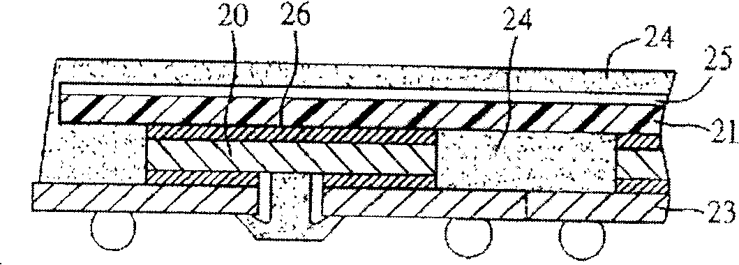
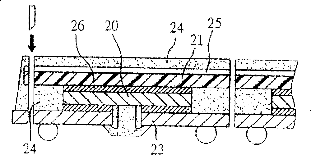
[0061] See Figure 6 As shown, it is a schematic cross-sectional view of Embodiment 3 of the semiconductor package structure made by the above-mentioned heat-dissipating package structure manufacturing method of the present invention. The packaging structure of the present invention includes: a chip carrier, a semiconductor chip, a heat sink, and a packaging colloid. The semiconductor package structure of the present invention is manufactured by a method similar to the preparation embodiment 1 and embodiment 2. The difference is that in the semiconductor package structure of the present embodiment, the heat sink connected to the semiconductor chip 61 63 is formed with an opening 63b at a position corresponding to the connecting chip 61, that is, at the position of the connecting chip 61, the thin metal layer 631 and the insulating core layer 630 on the lower surface of the heat sink 63 are removed, so as to be on the heat sink 63 An opening 63b exposing the thin metal layer 631 on...


PUM


Abstract

A heat-dissipating package structure and its manufacturing method. The package structure includes: a chip carrier, a semiconductor chip, a heat sink, and an encapsulant; it connects and electrically connects at least one semiconductor chip to the chip carrier, and connects the heat sink to the After the chip is mounted, the encapsulation and molding process is carried out, and the cutting process is performed along the periphery of the package component to reveal the side of the heat sink, and remove the encapsulant on the thin metal layer of the heat sink to expose the thin metal layer of the heat sink , the heat generated during operation is dissipated by the thin metal layer of the heat sink and the heat conduction through hole; the present invention avoids the problem of burrs and tool wear caused by cutting heat sinks with singling tools, and can also reduce the cutting cost in the singling process. Moreover, when the heat sink is integrated into the semiconductor structure, it will not cause chip cracks and glue overflow problems during the molding process, thereby improving the yield of finished products.

Description

Technical field [0001] The present invention relates to a heat-dissipating packaging structure and a manufacturing method thereof, in particular to a semiconductor packaging structure with a heat sink and a manufacturing method thereof. Background technique [0002] Ball grid array (Ball Grid Array, BGA) is an advanced semiconductor chip packaging technology, which is characterized by the use of a substrate to install the semiconductor chip, and on the back of the substrate to plant a number of solder balls arranged in a grid (Solder Ball), The semiconductor chip carrier of the same unit area can accommodate more input / output connections (I / O Connection) to meet the needs of highly integrated semiconductor chips. The entire package unit is soldered and electrically connected by these solder balls. Connect to an external printed circuit board. [0003] However, when a highly integrated semiconductor chip is in operation, it will be accompanied by a large amount of heat generation....

Claims


Application Information

Patent Timeline
Patent Type & Authority Patents(China)
IPC IPC(8): H01L21/50H01L23/31H01L23/34
CPCH01L24/97H01L2224/16225H01L2224/16245H01L2224/32225H01L2224/48091H01L2224/48227H01L2224/4824H01L2224/73215H01L2224/73253H01L2224/73265H01L2224/97H01L2924/181H01L2924/351H01L2924/00014H01L2924/00
Inventor 黄建屏赖正渊
Owner SILICONWARE PRECISION IND CO LTD
Why Eureka
Try Eureka