Heat radiation type packaging structure and its making method

A packaging structure and heat dissipation technology, applied in semiconductor/solid-state device manufacturing, electrical components, electric solid-state devices, etc., can solve the problems of high loss of stamping or cutting tools, inability to greatly improve production efficiency, and affect the appearance of packages, etc., to achieve Less wear and tear, good for cutting cost control, less prone to burrs

Inactive Publication Date: 2006-09-06
SILICONWARE PRECISION IND CO LTD
View PDF3 Cites 2 Cited by
  • Summary
  • Abstract
  • Description
  • Claims
  • Application Information

AI Technical Summary

Problems solved by technology

[0012] However, in the above-mentioned semiconductor package manufacturing process, when the singulation step is performed, because the singulation tool directly passes through the heat sink, and because the heat sink is generally made of a metal material with a hard texture and sufficient thickness, no matter whether it is used during singulation When punching or cutting with a diamond knife, the peripheral material of the heat sink will produce uneven sharp edges (or burrs) due to pulling, which will affect the appearance of the package, and will also cause excessive loss of punching or cutting tools , resulting in a substantial increase in cost, and the production efficiency cannot be greatly improved

Method used


Image

  • Heat radiation type packaging structure and its making method
  • Heat radiation type packaging structure and its making method
  • Heat radiation type packaging structure and its making method

Examples


Embodiment 1

[0043] see Figure 4A to Figure 4F , which is a schematic diagram of the manufacturing process of Embodiment 1 of the heat dissipation packaging structure manufacturing method of the present invention.

[0044] Such as Figure 4A and Figure 4B As shown, first, a matrix substrate module sheet 40A is provided, and the substrate module sheet 40A is formed by arranging a plurality of substrate units 40 in an array. The substrate unit 40 has an upper surface 400 and a lower surface 401 respectively, and defines a through hole 402 . The substrate units 40 can be arranged in a straight strip besides being arranged in an array, and a single substrate unit can also be used if the process conditions permit.

[0045] Next, at a predetermined position on the upper surface 400 of each substrate unit 40, the active surface 41a of the chip 41 is placed on it through an adhesive layer 45 such as silver glue, and the chip 41 is made to close the hole 402. At one end, a plurality of bondin...

Embodiment 2

[0052] Please refer to FIG. 5A to FIG. 5G , which are schematic diagrams of the manufacturing process of Embodiment 2 of the heat dissipation packaging structure manufacturing method of the present invention. The manufacturing process of Embodiment 2 of the present invention is substantially the same as that of Embodiment 1, the main difference being that the semiconductor chip in Embodiment 2 is flip-chip connected and electrically connected to the substrate.

[0053] Figure 5A and Figure 5BAs shown, first, a matrix substrate module sheet 50A is provided, and the substrate module sheet 50A is formed by arranging a plurality of substrate units 50 in an array. The substrate units 50 each have an upper surface 500 and a lower surface 501 . Wherein, the substrate units 50 can also be arranged in a straight strip besides being arranged in an array, and a single substrate unit can also be used if the process conditions permit.

[0054] Next, at a predetermined position on the up...

Embodiment 3

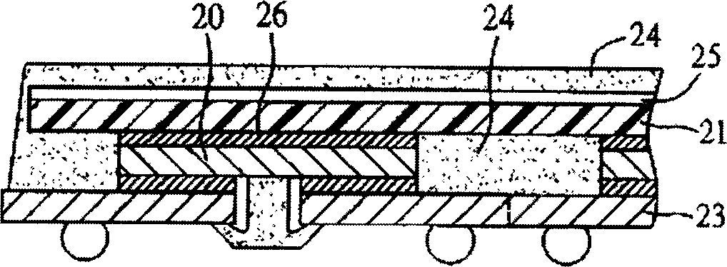
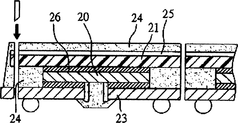
[0061] see Figure 6 As shown, it is a schematic cross-sectional view of Embodiment 3 of the semiconductor package structure manufactured by referring to the above heat-dissipating package structure manufacturing method of the present invention. The packaging structure of the present invention includes: a chip carrier, a semiconductor chip, a heat dissipation piece, and a packaging colloid. The semiconductor package structure of the present invention is made by a method similar to Preparation Example 1 and Example 2, the difference is that, in the semiconductor package structure of this embodiment, the heat sink connected to the semiconductor chip 61 63 is formed with an opening 63b at the position corresponding to the chip 61, that is, the metal thin layer 631 and the insulating core layer 630 part of the lower surface of the heat sink 63 are removed at the position of the chip 61, so that on the heat sink 63 Form the opening 63b that exposes the metal thin layer 631 on the ...


PUM


Abstract

A heat radiation type packaging structure and method of preparation, said packaging structure includes chip carrier, semiconductor chip, heat radiation piece and packaging colloid. It contains connecting at least one semiconductor chip on chip carrier, connecting heat radiation piece on said chip, to proceed packaging moulding process, cutting packaging assembly to expose side of said heat radiation piece, removing out packaging colloid on metallic film of heat radiation piece to expose metallic film, said metallic film and heat conduction through hole for radiating heat in operation. The present invention avoids chip rhegma and spillover glue problem in moulding process, and then raising finished goods rate.

Description

technical field [0001] The present invention relates to a heat dissipation packaging structure and a manufacturing method thereof, in particular to a semiconductor packaging structure with heat dissipation parts and a manufacturing method thereof. Background technique [0002] Ball Grid Array (BGA) is an advanced semiconductor chip packaging technology, which is characterized in that the semiconductor chip is placed on the substrate, and a plurality of grid-shaped solder balls (Solder Ball) are implanted on the back of the substrate. The semiconductor chip carrier of the same unit area can accommodate more input / output connection terminals (I / O Connection) to meet the needs of highly integrated semiconductor chips. The entire packaging unit is welded and electrically connected by these solder balls. connection to an external printed circuit board. [0003] However, when a highly integrated semiconductor chip is running, it will be accompanied by a large amount of heat gener...

Claims


Application Information

Patent Timeline
Patent Type & Authority Applications(China)
IPC IPC(8): H01L21/50H01L23/31H01L23/34
CPCH01L2224/73253H01L24/97H01L2924/0002H01L2224/4824H01L2224/48091H01L2224/16245H01L2224/16225H01L2224/73265H01L2224/48227H01L2224/73215H01L2224/32225H01L2224/97H01L2924/181H01L2924/351H01L2924/00014H01L2924/00
Inventor 黄建屏赖正渊
Owner SILICONWARE PRECISION IND CO LTD
Why Eureka
Try Eureka