Wave scalable InGaAs detector and array broadband buffering layer and window layer and its making method

A buffer layer and window layer technology, applied in semiconductor devices, final product manufacturing, sustainable manufacturing/processing, etc., can solve problems such as inability to realize windows, InP window layer mismatch, etc., to improve quantum efficiency and reduce surface recombination. , the effect of suppressing misfit dislocations

Inactive Publication Date: 2009-05-27
SHANGHAI INST OF MICROSYSTEM & INFORMATION TECH CHINESE ACAD OF SCI
View PDF4 Cites 0 Cited by
  • Summary
  • Abstract
  • Description
  • Claims
  • Application Information

AI Technical Summary

Problems solved by technology

For an In lattice-matched InP substrate 0.53 Ga 0.47 As detectors, people can use InP as the window layer, which avoids the lattice mismatch problem, and the effect is also very good, but for InP with extended wavelength x Ga 1-x As detectors have similar problems to the buffer layer: InP has a large mismatch as a window layer; InAs x P 1-x There are growth issues as a window layer; In x Ga 1-x As opaque cannot realize the function of the window

Method used


Image

  • Wave scalable InGaAs detector and array broadband buffering layer and window layer and its making method

Examples


Embodiment

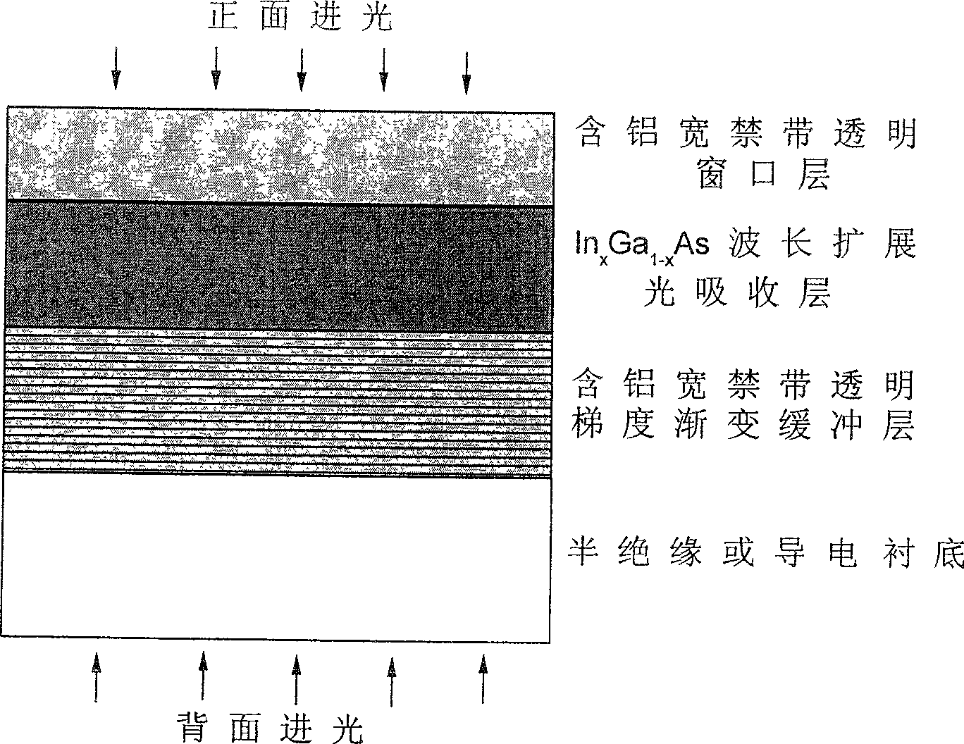
[0031] Embodiment: A wavelength-extended InGaAs photodetector array epitaxial material using InAlAs gradient gradient wide-bandgap transparent buffer layer and InAlAs wide-bandgap transparent window layer

[0032] Implementation steps:

[0033] 1. The cut-off wavelength of the InGaAs wavelength expansion detector array is required to be 2.5 μm (for the convenience of illustration, the following is taken as an example, the embodiment is not limited to 2.5 μm, and it can be extended to other wavelengths by analogy), so choose InGaAs light absorption The In composition of the layer is about 0.8;

[0034] 2. The material of the InGaAs wavelength expansion detector and its array can not only meet the requirements of the front light entrance, but also be suitable for the rear light entrance structure, so the semi-insulating InP single crystal with the [100] crystal orientation is used as the substrate;

[0035] 3. The detector adopts P on N (P-type material on top of N-type materia...


PUM


Abstract

The invention relates to a wide band transparent buffer layer and window layer which is used in wavelength expanding InGaAs photoelectricity detector and array and preparing method, it includes adopts material system which includes transparent grads shadow buffer structure which includes three aluminium or four aluminium which band width is bigger than wavelength expanding InGaAs material and adopts molecule beam extension method and easy to control, and can avoid miamatch and fits for back lighting, and transparent window layer structure which fits for light in front surface and decreases complex of surface and increases efficiency of quanta. The wide band buffer layer and window layer structure in the invention fits for unit or array which adopts back lighting and inversed encapsulated structure, also unit or array which adopts normal front lighting, it possesses perfect currency.

Description

technical field [0001] The invention relates to a wavelength extension InGaAs detector, an array broadband buffer layer and a window layer and a manufacturing method, more precisely to a wavelength extension InGaAs detector x Ga 1-x As (0.53<x<1) photodetector and wide bandgap transparent buffer layer and window layer structure and realization method of the array thereof, the invention belongs to the field of semiconductor optoelectronic materials and devices. Background technique [0002] In lattice-matched InP substrate 0.53 Ga 0.47 As ternary materials have the characteristics of direct bandgap and high electron mobility. Its forbidden band width at room temperature is about 0.75eV, and the corresponding wavelength is about 1.65μm, which can just cover the optical fiber communication band. Therefore, In 0.53 Ga 0.47 Photodetectors made of As ternary materials have been widely used in the field of optical communication, and also have important applications in rem...

Claims


Application Information

Patent Timeline
Patent Type & Authority Patents(China)
IPC IPC(8): H01L31/0304H01L31/18
CPCY02P70/50
Inventor 张永刚顾溢田招兵
Owner SHANGHAI INST OF MICROSYSTEM & INFORMATION TECH CHINESE ACAD OF SCI
Why Eureka
Try Eureka