Patterned sapphire substrate, preparation method thereof and LED epitaxial wafer
A patterned sapphire and patterned technology, which is applied to electrical components, circuits, semiconductor devices, etc., can solve the problem that the light extraction efficiency is difficult to further improve, and achieve the effects of increasing light scattering, strong operability, and increasing the probability of emission
- Summary
- Abstract
- Description
- Claims
- Application Information
AI Technical Summary
Problems solved by technology
Method used
Image
Examples
preparation example Construction
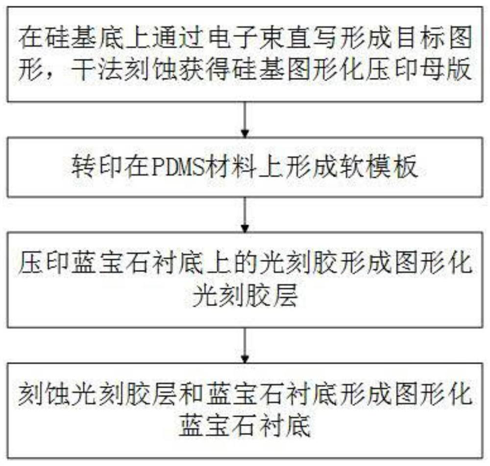
[0071] The present invention also provides a method for preparing a patterned sapphire substrate described above, comprising the steps of:
[0072] (a) Coating embossing photoresist on the sapphire flat sheet, using a soft template to carry out an embossing process on the sapphire flat sheet coated with the imprinting photoresist to form a patterned photoresist layer;
[0073] (b) Etching the sapphire flat sheet forming the patterned photoresist layer by an ICP dry etching process to obtain a patterned sapphire substrate;
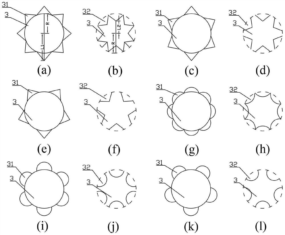
[0074] Wherein, the pattern of the patterned photoresist layer includes periodically arranged circles and several protruding parts or concave parts arranged periodically along the circumference of the circles along the plan view direction.
[0075] The preparation method of the present invention can obtain a patterned sapphire substrate with regular edges and corners through the design of mask patterns and the like. The presence of edges and corners can fu...
Embodiment 1
[0090] This embodiment provides a method for preparing a patterned sapphire substrate, and the process roadmap and schematic diagram refer to image 3 and Figure 4 , including the following steps:
[0091] (1) Preparation of graphic imprint master
[0092] First, it is formed on the imprinted hard master by electron beam direct writing, such as Figure 5 The target pattern shown is then subjected to dry etching to obtain a patterned imprint master. Wherein, the imprinted hard master is preferably a silicon substrate.
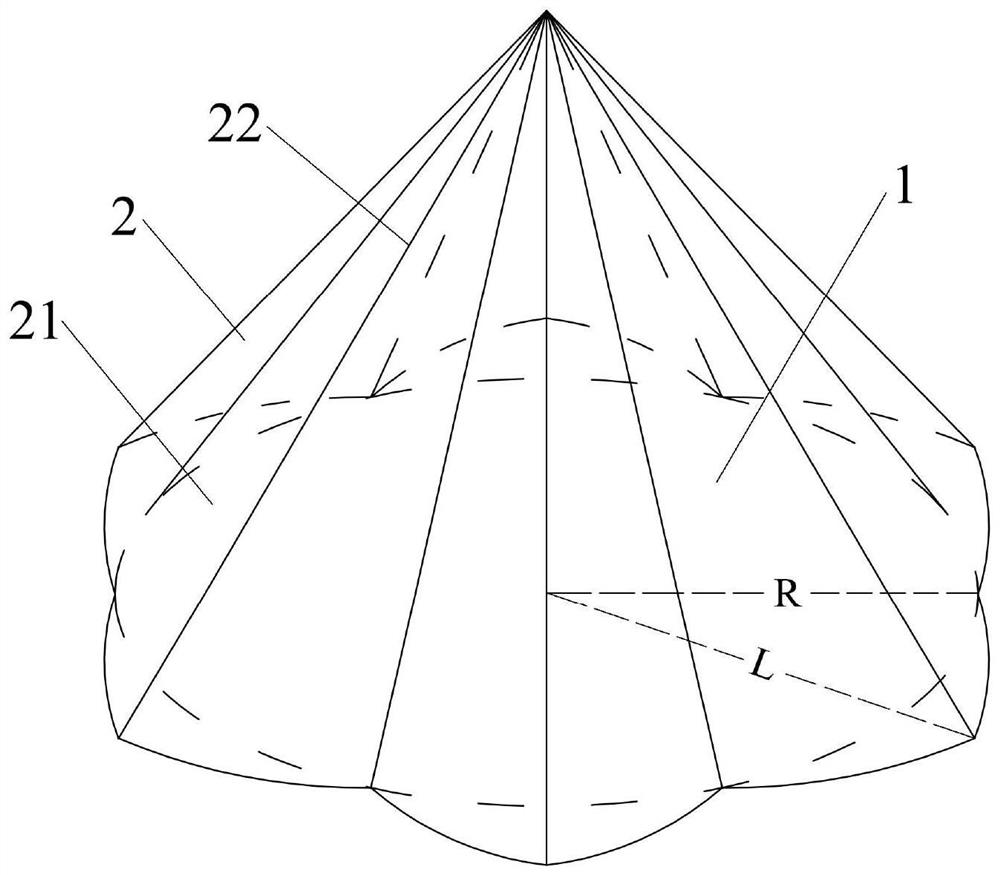
[0093] The target figure includes a circle and 5 fan-like protrusions of the same size arranged periodically along the circumference of the circle (enclosed by arc-shaped edges and circular parts), adjacent to the fan-like The protruding parts are connected end to end in sequence, the radius of the circle is R, the distance from the farthest end of the circular arc in the fan-like shape to the center of the circle is L, and satisfy: L≤1.5R ; Wherein, the n...
Embodiment 2
[0103] This embodiment refers to the preparation method of Example 1, the only difference is that the target pattern is different. Target graphic reference for this example figure 2 (i) in.
[0104] The target graphics are not limited to this, you can also refer to figure 2 The rest of the target graphics.
[0105] The patterned sapphire substrate of the present invention has certain regular edges and corners, which can change the traveling direction of the light emitted by the LED active area, so that more light can meet the emission conditions, thereby improving the light extraction efficiency.
PUM
| Property | Measurement | Unit |
|---|---|---|
| diameter | aaaaa | aaaaa |
| thickness | aaaaa | aaaaa |
Abstract
Description
Claims
Application Information


