
Display pixel structure and display device

A technology for display pixels and display devices, which is applied in the direction of using solid-state color display device image reproducers, identification devices, image/graphic display tubes, etc., can solve the problems of power consumption, increased cost, large energy loss, etc. The effect of efficiency

Inactive Publication Date: 2010-03-10
IND TECH RES INST
View PDF6 Cites 0 Cited by
  • Summary
  • Abstract
  • Description
  • Claims
  • Application Information

AI Technical Summary

Problems solved by technology

In addition, because the luminous mechanism of gas discharge undergoes two processes to emit visible light, the energy loss is relatively large. If plasma needs to be generated during the process, it will consume more power.
On the other hand, a field emission light source needs to grow or coat a uniform electron-emitting end on the cathode, but the technology for large-scale production of this type of cathode structure is not yet mature, and the uniformity of the electron-emitting end and the production yield are not good. bottleneck
In addition, the distance between the cathode and anode of the field emission light source needs to be controlled accurately, and the packaging of ultra-high vacuum is difficult, which also relatively increases the production cost

Method used


Image

  • Display pixel structure and display device
  • Display pixel structure and display device
  • Display pixel structure and display device

Examples


Embodiment Construction

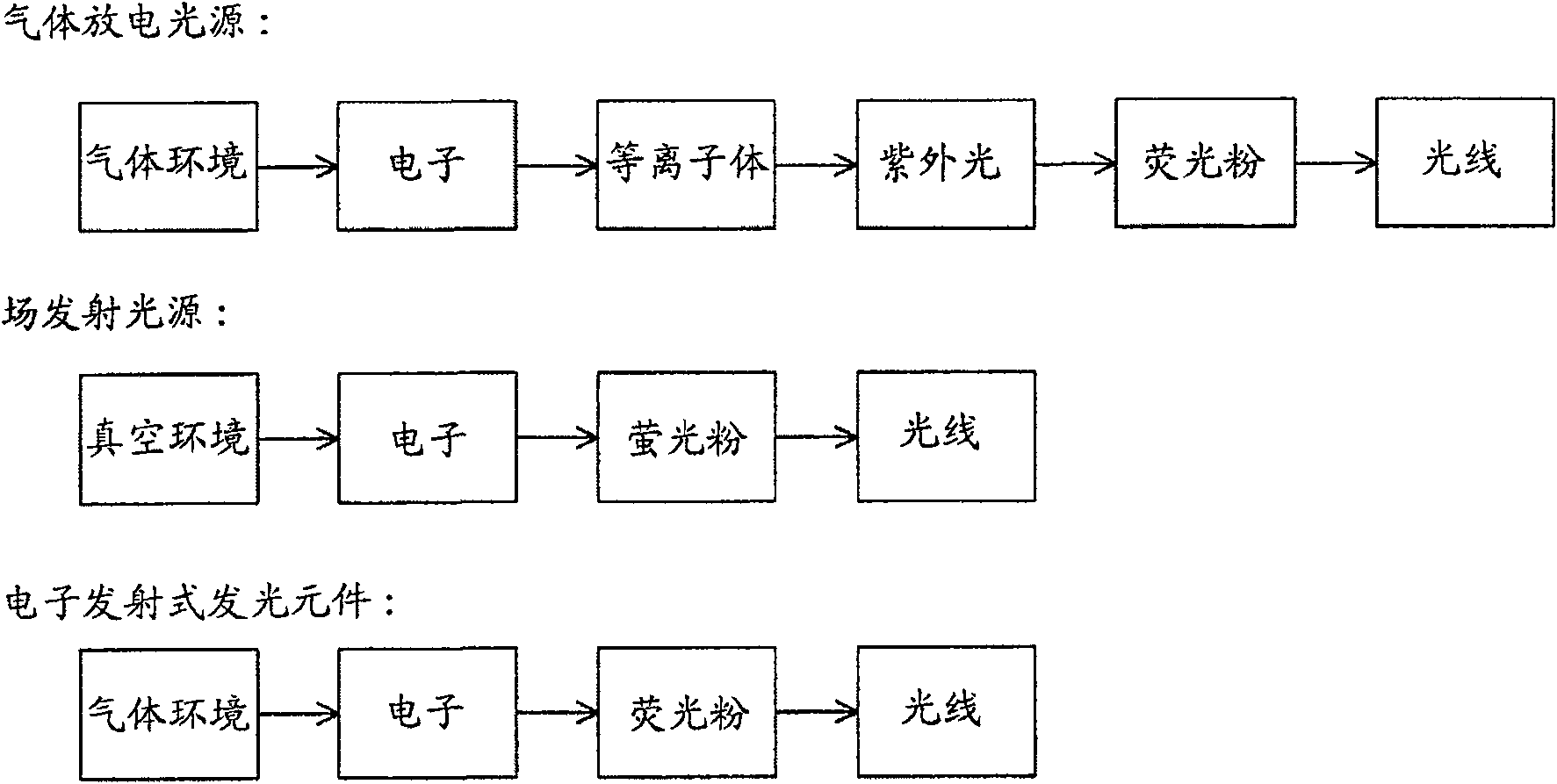
[0046] The electron-emitting light-emitting element proposed by the present invention has both the advantages of the traditional gas discharge light source and the field emission light source, and overcomes the shortcomings of the two traditional light-emitting structures. Please refer to figure 1 A comparison diagram of the light-emitting mechanism of the above-mentioned two traditional light-emitting structures and the electron-emitting light-emitting device of the present invention is shown. In more detail, the known gas glow discharge light source uses the electric field between the cathode and the anode to dissociate the gas filled in the discharge chamber, and through the conduction of the gas, electrons collide with other gas molecules to generate ultraviolet light, while fluorescence The layer absorbs ultraviolet light and emits visible light. In addition, the known field emission light source is in an ultra-high vacuum environment, and the high aspect ratio structure...


PUM


Abstract

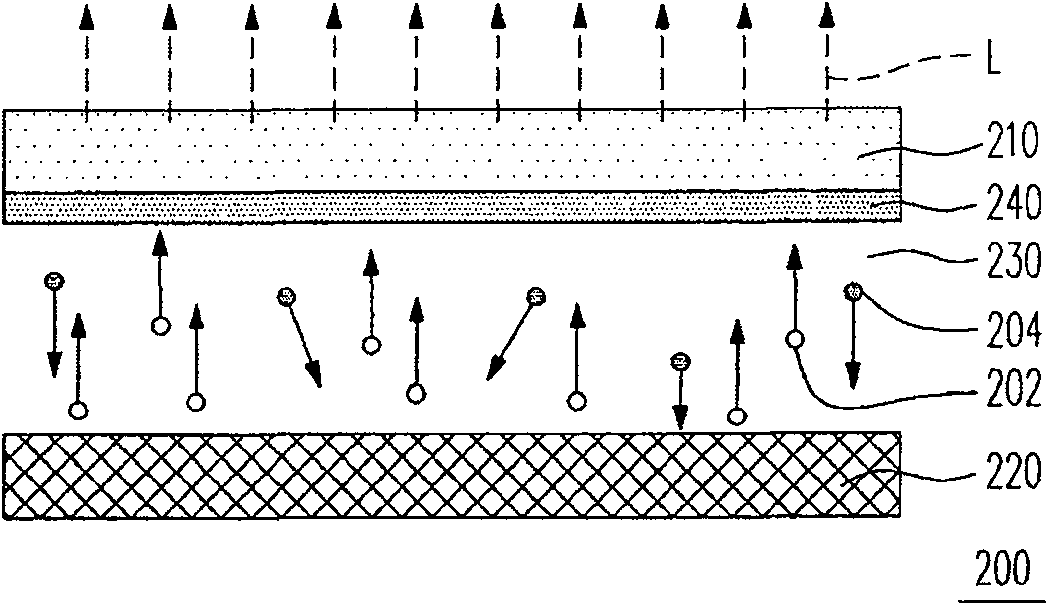
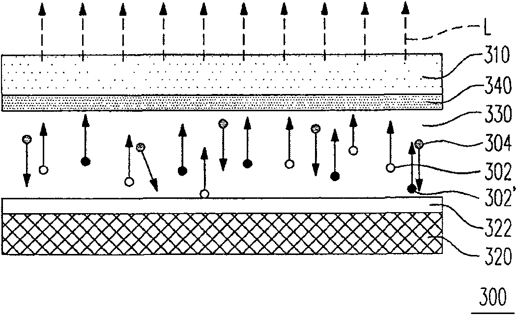
The invention discloses a display pixel structure and display apparatus. The pixel structure of display apparatus includes a first substrate and a second substrate. Several cathode structure layers are disposed on the first substrate. The second substrate is a light-transmissive material. Several anode structure layers are disposed on the second substrate, and are light-transmissive conductive materials. The first substrate faces to the second substrate, so that the cathode structure layers are respectively aligned with the anode structure layers. A separation structure is disposed between thefirst substrate and the second substrate, for respective partitioning the anode structure layers and the cathode structure layers to form several spaces. Several fluorescent layers are respectively disposed between the anode structure layers and the cathode structure layers. A low-pressure gas is respectively filled into the spaces. The low-pressure gas has an electron mean free path, allowing atleast sufficient amount of electrons to directly impinge the fluorescent layer under an operation voltage.

Description

technical field [0001] The invention relates to a light-emitting element, and in particular to an electron-emitting light-emitting element and its application. Background technique [0002] Two types of light-emitting structures are mainly used in mass-produced light source devices or display devices, including: [0003] 1. Gas discharge light source: applied to plasma panels or gas discharge lamps, mainly using the electric field between the cathode and the anode to dissociate the gas filled in the discharge chamber, and make the electrons After impacting the gas, a transition occurs and emits ultraviolet light, while the fluorescent layer also located in the discharge cavity absorbs ultraviolet light and emits visible light. [0004] 2. Field emission light source: used in field emission displays such as carbon nanotubes, etc., mainly to provide an ultra-high vacuum environment, and to make electron emitters of nano-carbon materials on the cathode to utilize the electron ...

Claims


Application Information

Patent Timeline
Patent Type & Authority Patents(China)
IPC IPC(8): H01J31/15H01J31/12H01J29/94H01J29/08H01J29/02H01J29/04H01J29/20G09F9/30H04N11/00
CPCH01J61/62H01J63/08
Inventor 李中裕陈世溥林依萍林韦至卓连益
Owner IND TECH RES INST
Learn More