An a-Si:H solar battery with the boron mixing non-crystal diamond film as the window layer and its making method

An amorphous diamond and solar cell technology, which is applied in the field of amorphous silicon solar cells and their preparation, can solve the problems of low conversion efficiency of p-type amorphous silicon layer solar cells and the like, and achieves good doping properties and wide transmittance. , the effect of high hardness

Inactive Publication Date: 2007-08-01
HARBIN INST OF TECH
View PDF0 Cites 8 Cited by
  • Summary
  • Abstract
  • Description
  • Claims
  • Application Information

AI Technical Summary

Problems solved by technology

[0004] The purpose of the present invention is to solve the problem of low conversion efficiency of existing p-type amorphous silicon

Method used


Image

  • An a-Si:H solar battery with the boron mixing non-crystal diamond film as the window layer and its making method
  • An a-Si:H solar battery with the boron mixing non-crystal diamond film as the window layer and its making method

Examples


specific Embodiment approach 1

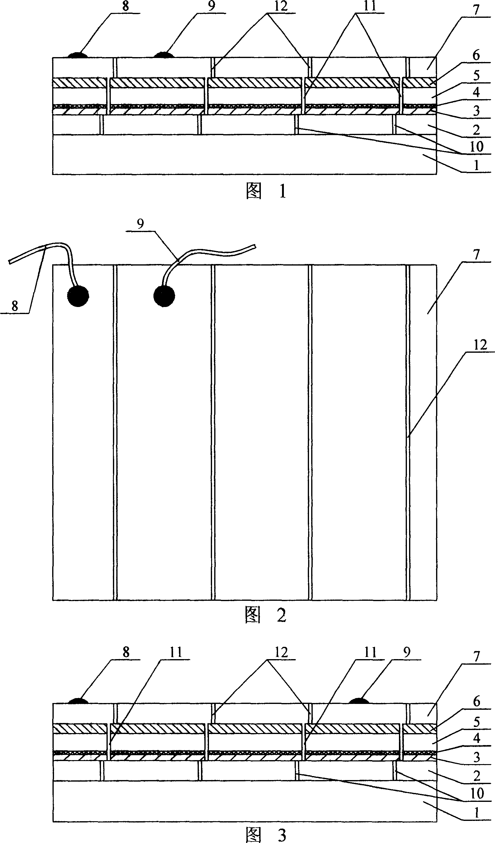
[0016] Specific Embodiment 1: (See Figures 1 to 3) In this embodiment, the a-Si:H solar cell with boron-doped amorphous diamond film as the window layer is formed from bottom to top by Corning glass 1, SnO 2 :F conductive film 2, p-ta-C:B film 3, transition p-a-Si:H(C) film 4, i-a-Si:H film 5, n-a-Si:H film 6, aluminum film 7, anode connection 8 and cathode wiring 9; SnO 2 :F conductive film 2 has laser scribed lines 10 with an interval of 10±0.3mm, p-ta-C:B film 3, transition p-a-Si:H(C) film 4, i-a-Si:H film 5 And n-a-Si: H thin film 6 has the first silicon scribe line 11 that is parallel to the direction of laser scribe line 10 and the spacing with laser scribe line 10 is 1 ± 0.1mm; The direction of the line 11 is parallel to the second silicon scribe line 12 with a distance of 1 ± 0.1mm from the first silicon scribe line 11, the upper end surface of the Corning glass 1 and the SnO 2 : The lower end surface of F conductive film 2 is fixedly connected, SnO 2 : The upper e...

specific Embodiment approach 2

[0017] Embodiment 2: In this embodiment, there are five second silicon scribe lines 12 between the anode wire 8 and the cathode wire 9 . Others are the same as in the first embodiment.

specific Embodiment approach 3

[0018] Embodiment 3: In this embodiment, there are ten second silicon scribe lines 12 between the anode wire 8 and the cathode wire 9 . Others are the same as in the first embodiment.


PUM

PropertyMeasurementUnit
Thicknessaaaaaaaaaa
Thicknessaaaaaaaaaa
Thicknessaaaaaaaaaa

Abstract

The a-Si:H solaode and preparing method which regards the boron-doping amorphous diamond film as window layer, it relates to a amorphous silicon solaode and preparing method. It resolves the problems of low transform efficiency of current p type amorphous silicon solaode. The upper surface of the corning glass (1) is connected with the lower surface of the SnO2:F conducting film (2), the upper surface of the SnO2:F conducting film (2) is connected with the lower surface of the p-ta-C:B film (3), the upper surface of the p-ta-C:B film (3) is connected with the lower surface of the transition p-a-Si:H(C) film (4), the upper surface of the transition p-a-Si:H(C) film (4) is connected with the lower surface of the i-a-Si:H film (5), the upper surface of the i-a-Si:H film (5) is connected with n-a-Si:H film (6). The method of the invention possesses following steps: a. depositing the SnO2:F conducting film, b. scoring with laser, c. depositing p-ta-C:B film, d. depositing transition p-a-Si:H(C) film, i-a-Si:H film and n-a-Si:H film, e. scoring with silicon firstly, f. evaporation of aluminum, g. scoring with silicon secondly. The invention possesses advantages of increasing transform efficiency of battery.

Description

technical field [0001] The invention relates to an amorphous silicon solar cell and a preparation method thereof. Background technique [0002] With the increasingly serious energy crisis and environmental pollution, the development of renewable clean energy has gradually become one of the major international strategic issues. Solar energy is an inexhaustible clean energy source, therefore, the development and utilization of solar energy has become a strategic decision for sustainable development in the energy field of countries all over the world. According to different materials, solar cells are mainly divided into: monocrystalline silicon solar cells, polycrystalline silicon solar cells, amorphous silicon solar cells, II-VI polycrystalline thin-film solar cells and III-V compound solar cells. Among them, traditional crystalline silicon solar cells and semiconductor compound solar cells have always occupied an important position in the market due to their high conversion ...

Claims


Application Information

Patent Timeline
IPC IPC(8): H01L31/075H01L31/042H01L31/20H01L31/0352
CPCY02E10/50Y02E10/548Y02P70/50
Inventor 韩杰才朱嘉琦檀满林
Owner HARBIN INST OF TECH
Why Eureka
Try Eureka