Exposure device, exposure method, and device manufacture method
An exposure device and scanning exposure technology, which are applied in semiconductor/solid-state device manufacturing, photolithography exposure devices, microlithography exposure equipment, etc., can solve the problem of equipment that may be attached to the equipment that constitutes the exposure device, and the accuracy of the transfer pattern deteriorates , measurement accuracy deterioration, etc.
- Summary
- Abstract
- Description
- Claims
- Application Information
AI Technical Summary
Problems solved by technology
Method used
Image
Examples
no. 1 approach
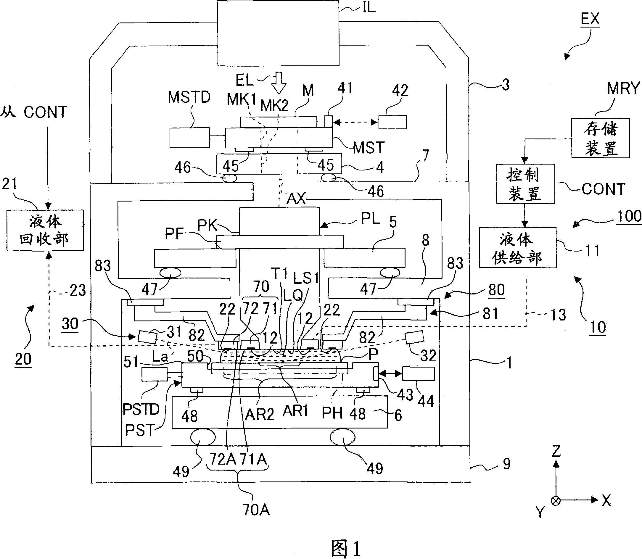
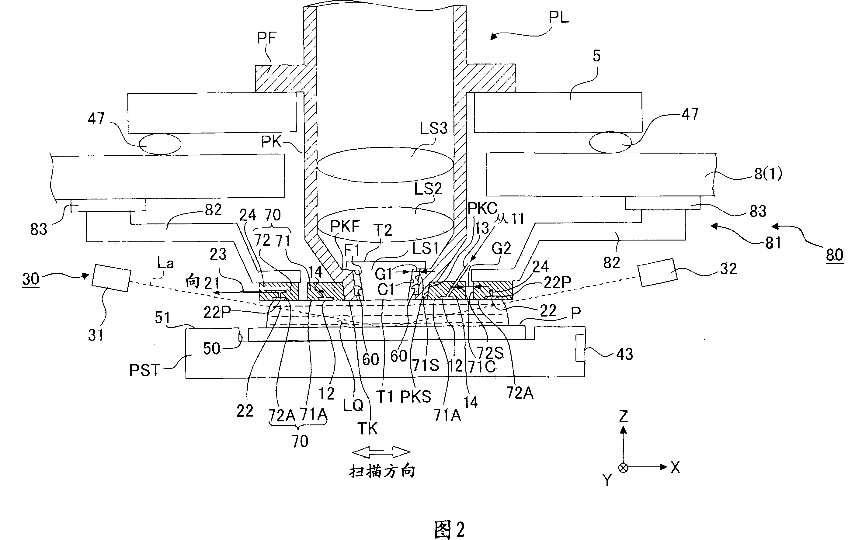
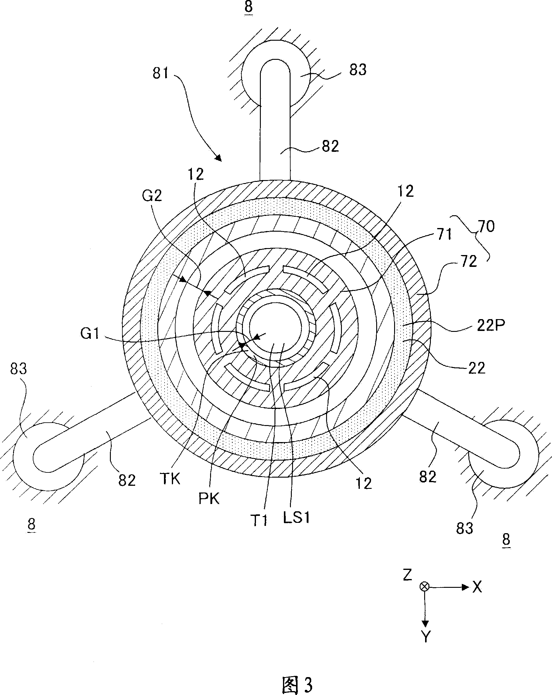
[0036] FIG. 1 is a schematic configuration diagram showing an exposure apparatus EX according to a first embodiment. In FIG. 1 , the exposure apparatus EX includes: a mask stage MST that can move while holding a mask M; a substrate stage PST that can move while holding a substrate P; an illumination optical system IL that The mask M held on the mask stage MST is illuminated with the exposure light EL; the projection optical system PL projects and exposes the pattern image of the mask M illuminated by the exposure light EL onto the substrate stage. The substrate P of the PST; and the control device CONT, which uniformly controls the action of the entire exposure device EX. The storage device MRY that stores information related to exposure processing is connected to the control device CONT.
[0037] The exposure apparatus EX of this embodiment is a liquid immersion exposure apparatus that substantially shortens the exposure wavelength to improve resolution, and uses a liquid im...
no. 2 approach
[0092] Next, a second embodiment of the present invention will be described with reference to FIG. 6 . However, in the following description, the same reference numerals are assigned to the same or equivalent components as those of the above-mentioned embodiment, and the description thereof will be omitted or simplified.
[0093] The characteristic part of the second embodiment is that the nozzle member 70 is composed of a single member, and the supply port 12 for supplying the liquid LQ and the recovery port 22 for recovering the liquid LQ are respectively provided on the lower surface 70A of the nozzle member 70 . In FIG. 6 , nozzle member 70 is an annular member formed to surround projection optical system PL, and a predetermined gap G3 is provided between outer surface PKC of barrel PK of projection optical system PL and inner surface 70S of nozzle member 70 . This gap G3 prevents the vibration of the nozzle member 70 from being directly transmitted to the projection optic...
no. 3 approach
[0095] Next, a third embodiment of the present invention will be described with reference to FIG. 7 . The difference between the third embodiment and the first embodiment, that is, the characteristic part of the third embodiment, is that the supply port 12 for supplying the liquid LQ is provided on the lower surface TK of the lens barrel PK, and the supply port 12 and the supply pipe 13 are connected. The internal flow path 14 is provided on the lens barrel PK. That is, in this embodiment, the lens barrel PK holding the optical element LS1 constituting the projection optical system PL includes the first nozzle member 71 for supplying the liquid LQ. Further, a second nozzle member 72 is provided around the lens barrel PK having this supply port 12 . The second nozzle member 72 has a recovery port 22 on its lower surface 72A, and is supported by the lower stepped portion 8 of the main frame 1 via a support mechanism 81 . The second nozzle member 72 is an annular member formed ...
PUM
 Abstract
Description
Claims
Application Information


