Flat-plate sandwich structural semiconductor type gas sensor and producing method thereof
A gas sensor and sandwich structure technology, which is applied in semiconductor/solid-state device manufacturing, electrical components, circuits, etc., can solve the problems of low manufacturing process precision, high heating power consumption, low electrical conductivity, etc., and achieve high manufacturing process precision and signal. Strong, small output resistance effect
- Summary
- Abstract
- Description
- Claims
- Application Information
AI Technical Summary
Problems solved by technology
Method used
Image
Examples
specific Embodiment approach 1
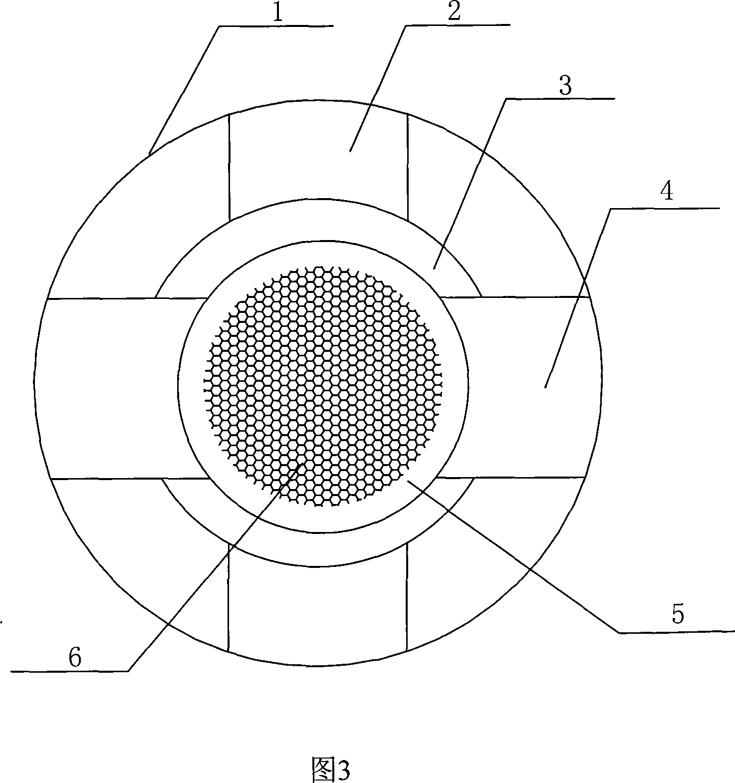
[0018] Specific Embodiment 1: The present embodiment will be specifically described below in conjunction with FIG. 1, FIG. 2 and FIG. , the substrate 1, the heater 2, the insulating isolation layer 3, the sensitive electrode 4, the sensitive film 5 and the porous electrode 6 are concentric and in a regular shape, and the heater 2 is etched on the substrate 1, and the heater The length of 2 is equal to the diameter of the substrate 1, and an insulating isolation layer 3 is plated on the heater 2, and a sensitive electrode 4 is etched on the insulating isolation layer 3, and the length of the sensitive electrode 4 is equal to the diameter of the substrate 1, and the sensitive electrode 4 and the heater 2 are perpendicular to each other, the area of the insulating isolation layer 3 is larger than the area of the overlapping part of the heater 2 and the sensitive electrode 4, the area of the insulating isolation layer 3 is smaller than the area of the substrate 1, and the s...
specific Embodiment approach 2
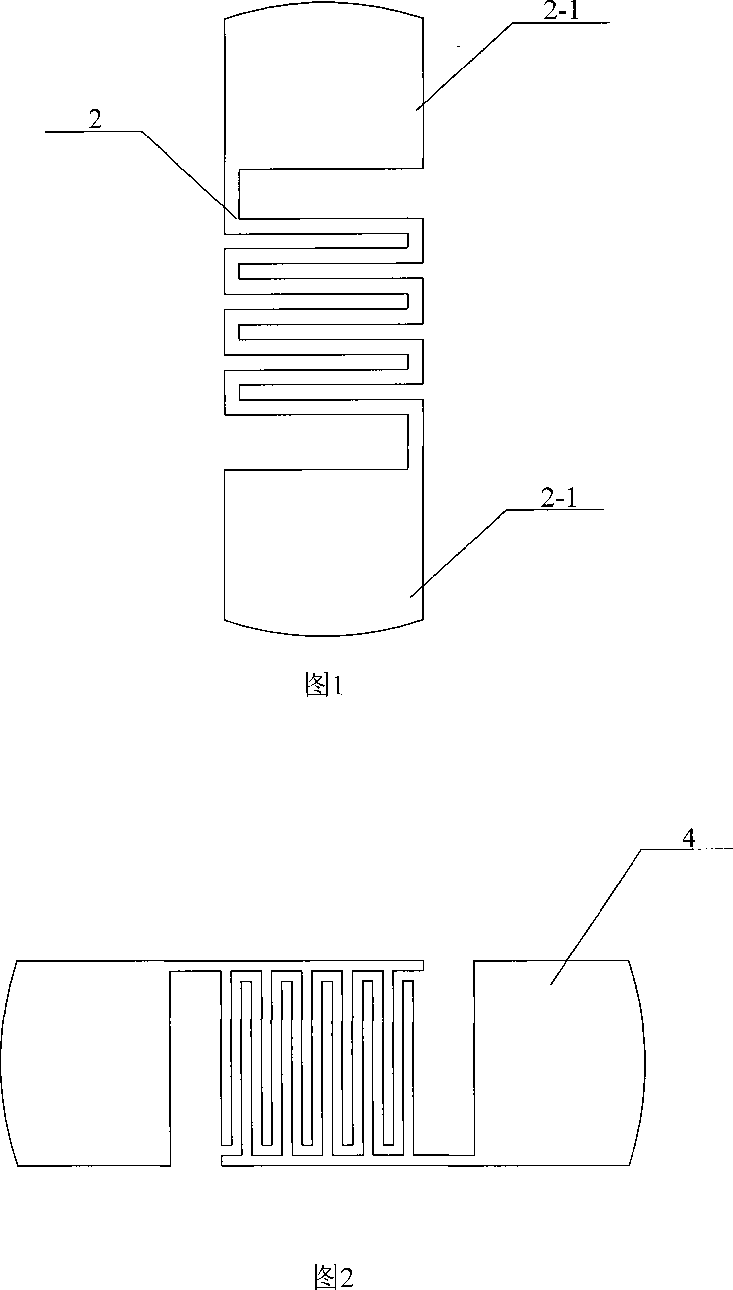
[0019] Specific Embodiment 2: The present embodiment will be described in detail below in conjunction with FIG. 1. In this embodiment, the middle part of the heater 2 is serpentine, and the two sides are pads 2-1, and the pads 2-1 on both sides are equal in size. Other components And the connection relationship is the same as the specific embodiment one.
specific Embodiment approach 3
[0020] Specific embodiment three: the present embodiment is described in detail below, and the present embodiment has the following steps to complete
[0021] Step 1: Select the required substrate, the substrate is SiO with a thickness of 0.1-0.5mm 2 / Si, Ai 2 o 3 Or glass, and then boiled with deionized water for 10-20 minutes to wash away the soluble pollutants on the substrate, and then ultrasonically cleaned with acetone at a frequency of 30khz for 10-20min to remove organic pollutants on the substrate, and then used alcohol at a frequency of 30khz Perform ultrasonic cleaning for 10-20 minutes to wash away organic pollutants on the substrate, and use deionized water to perform ultrasonic cleaning at a frequency of 30khz for 10-20 minutes. Dry or dry the substrate to wash away the acetone and alcohol remaining on the substrate;
[0022] Step 2: To make the heater, follow the steps below:
[0023]Operation sequence 1: Put the substrate into the sampling chamber of the JG...
PUM
| Property | Measurement | Unit |
|---|---|---|
| thickness | aaaaa | aaaaa |
Abstract
Description
Claims
Application Information

