
Light emitted semiconductor assembly package structure and producing method thereof

A technology of light-emitting semiconductors and packaging structures, which is applied in semiconductor/solid-state device manufacturing, semiconductor devices, semiconductor/solid-state device components, etc. It can solve problems such as uneven color temperature and precipitation, achieve uniform color temperature, avoid gaps, and reduce manufacturing costs Effect

Inactive Publication Date: 2007-08-22
EVERLIGHT ELECTRONICS
View PDF0 Cites 5 Cited by
  • Summary
  • Abstract
  • Description
  • Claims
  • Application Information

AI Technical Summary

Problems solved by technology

The phosphor colloid fixing structure can control the shape and thickness of the phosphor colloid coating layer, and solve the problem that the phosphor colloid is deposited on the edge of the light emitting semiconductor component in the traditional light-emitting semiconductor component packaging structure, which causes the fluorescent powder colloid to pass through the top of the phosphor colloid coating layer. The problem of uneven color temperature caused by the different lengths of light paths between the surface and the side

Method used

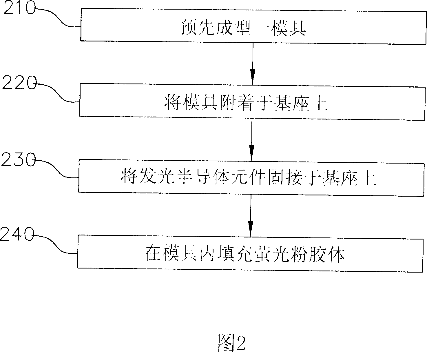
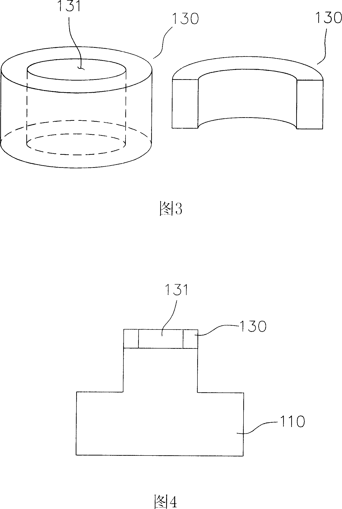

Image

  • Light emitted semiconductor assembly package structure and producing method thereof
  • Light emitted semiconductor assembly package structure and producing method thereof
  • Light emitted semiconductor assembly package structure and producing method thereof

Examples


Embodiment Construction

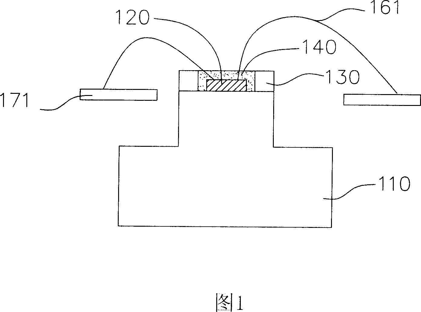
[0028] Please refer to FIG. 1 , which shows a cross-sectional view of a packaging structure of a light-emitting semiconductor device of the present invention. The packaging structure 100 of light-emitting semiconductor components includes a substrate 110 , a light-emitting semiconductor component 120 , a phosphor colloid fixing structure 130 and a phosphor colloid coating layer 140 .

[0029] The light-emitting semiconductor component 120 and the phosphor colloid fixing structure 130 are disposed on the base 110; wherein, the phosphor colloid fixing structure 130 has an opening and surrounds the light-emitting semiconductor component 120, and the metal wire 161 is electrically connected to the light-emitting semiconductor component 120 between the positive and negative electrodes and the electric energy input electrode 171. The phosphor colloid coating layer 140 is filled in the phosphor colloid fixing structure 130 through the opening of the phosphor colloid fixing structure ...


PUM


Abstract

This invention relates to a package structure of light-emitting semiconductor components including a base, a light-emiting semiconductor component, a a phosphor powder colloid fixing structure and a phosphor powder colloid cover, in which, the semiconductor component is set on the base, the highly transmitted phosphor powder colloid fixing structure is set on the base surrounding the component and opened with an opening on the top and the colloid is filled into the structure through the opening to cover the light emission semiconductor component to form a cover of the phosphor powder colloid.

Description

technical field [0001] The present invention relates to a packaging structure of a light-emitting semiconductor component and a manufacturing method thereof, and in particular relates to a fluorescent powder with a mold-free design that is suitable for the packaging structure of a light-emitting semiconductor component and can precisely control the shape and size of the fluorescent powder colloid. Light powder laying method. Background technique [0002] In today's light-emitting diode (LED) industry, phosphor powder is widely used in the packaging technology of white light, warm color light and pink light-emitting semiconductor components. [0003] Taking white light-emitting diodes as an example, fluorescent powder colloid is traditionally made by mixing phosphor powder and colloid. It is dropped on light-emitting semiconductor components by dispensing equipment, and the blue light emitted by blue light-emitting diodes excites yellow phosphor powder to produce Yellow ligh...

Claims


Application Information

Patent Timeline
Patent Type & Authority Applications(China)
IPC IPC(8): H01L33/00H01L23/31H01L21/56H01L33/52
CPCH01L2224/8592H01L2224/48091H01L2224/48247
Inventor 吴易座庄世任张嘉显周大为
Owner EVERLIGHT ELECTRONICS
Learn More