Semiconductor transistor element and its production

A technology of transistors and MOS transistors, applied in the field of N or P-type metal-oxide-semiconductor field-effect transistors and their production, can solve the problems of unsatisfactory and limited transistors, etc.

Active Publication Date: 2007-09-05
UNITED MICROELECTRONICS CORP
View PDF0 Cites 17 Cited by
  • Summary
  • Abstract
  • Description
  • Claims
  • Application Information

AI Technical Summary

Problems solved by technology

For example, in the prior art, in order to improve the performance of the transistor, the silicon nitride capping layer 46 covering the silicon nitride spacer 32 is usually provided with a stress, such a...

Method used


Image

  • Semiconductor transistor element and its production
  • Semiconductor transistor element and its production
  • Semiconductor transistor element and its production

Examples


Embodiment Construction

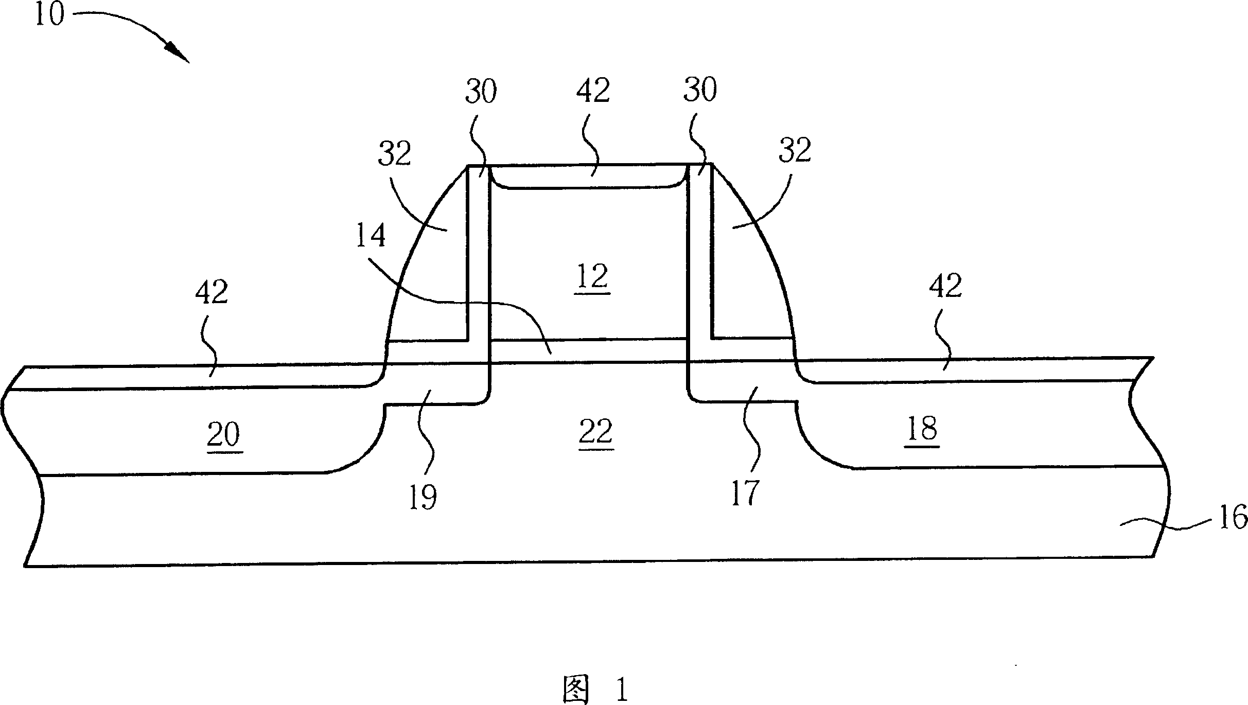
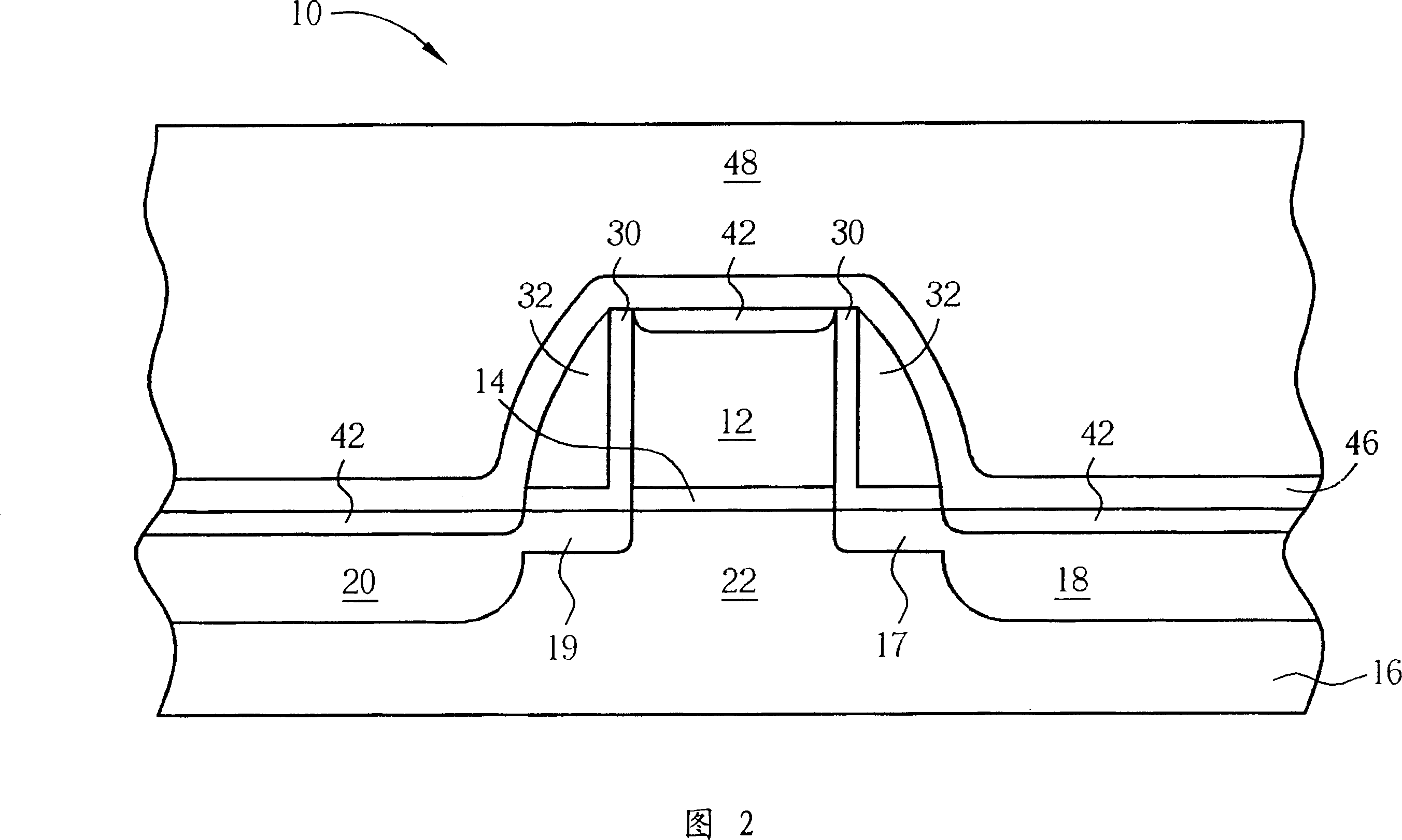
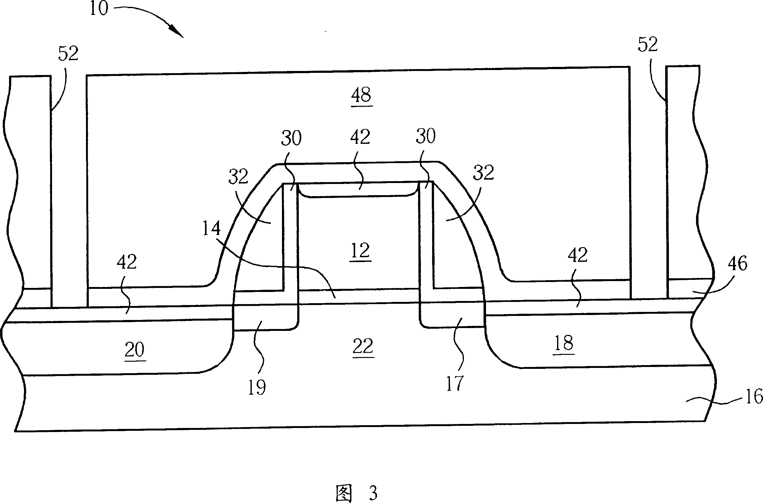
[0057] Please refer to FIG. 4 to FIG. 11 , which are schematic cross-sectional views of the method for manufacturing semiconductor MOS transistor elements 10 and 100 according to a preferred embodiment of the present invention, wherein the same elements or parts are still represented by the same symbols. It should be noted that the drawings are for illustrative purposes only and are not drawn to scale. In addition, in FIGS. 4 to 11 , the photolithography and etching processes for the parts related to the present invention are well known to those skilled in the art, so they are not explicitly shown in the drawings.

[0058] The present invention relates to a method for fabricating MOS transistor elements or CMOS elements in an integrated circuit. In FIGS. 4 to 11 , the CMOS process is particularly used as an illustration. First, as shown in FIG. 4 , a semiconductor substrate including a silicon layer 16 is prepared, wherein the region 1 is used to fabricate the NMOS device 10 ,...


PUM

PropertyMeasurementUnit
Thicknessaaaaaaaaaa
Thicknessaaaaaaaaaa

Abstract

The invention is concerned with the method of making metal oxide semiconductor (MOS)transistor element, the characteristic is: the back-etching step that uses the silicon nitride covering layer with different stress and the superfluity shallow gully insulating layer, the field effect transistor element of N or P metal oxide semiconductor can with higher current gain, improves the operating efficiency of the semiconductor transistor element.

Description

technical field [0001] The invention relates to a semiconductor transistor element and a manufacturing method thereof, in particular to an N or P-type metal-oxide-semiconductor (MOS) field effect device without a silicon nitride spacer-less (silicon nitride spacer-less) Transistor element and method of making the same. Background technique [0002] As known in the industry, current high-speed metal-oxide-semiconductor transistor devices with strained silicon use the principle that the lattice constant of the silicon germanium layer is different from that of silicon, resulting in structural strain when silicon is epitaxy on silicon germanium. . In this type of strained Si-FET device, a biaxial tensile strain of the Si layer is usually involved, due to the fact that the SiGe layer has a larger lattice constant than Si, which makes The band structure of silicon is changed, resulting in increased carrier mobility. Therefore, a component with a strained silicon structure in th...

Claims


Application Information

Patent Timeline
IPC IPC(8): H01L21/336H01L21/8238H01L29/78H01L27/092
Inventor 丁世汎黄正同洪文瀚郑子铭沈泽民盛义忠
Owner UNITED MICROELECTRONICS CORP
Why Eureka
Try Eureka