Theta-doped 4HSiC avalanche ultraviolet photoelectric detector and its production

A technology of electrical detectors and ultraviolet light, applied in circuits, electrical components, semiconductor devices, etc., can solve problems such as response time, quantum efficiency, and breakdown voltage that cannot reach optimal values

Inactive Publication Date: 2007-09-05
XIAMEN UNIV
View PDF0 Cites 25 Cited by
  • Summary
  • Abstract
  • Description
  • Claims
  • Application Information

AI Technical Summary

Problems solved by technology

A good optimal value cannot be reached among the response time, quantum efficiency and breakdown voltage of the device
The present invention adopts the avalanche photodetector structure that separates the absorption region, the charge re

Method used


Image

  • Theta-doped 4HSiC avalanche ultraviolet photoelectric detector and its production

Examples


Embodiment Construction

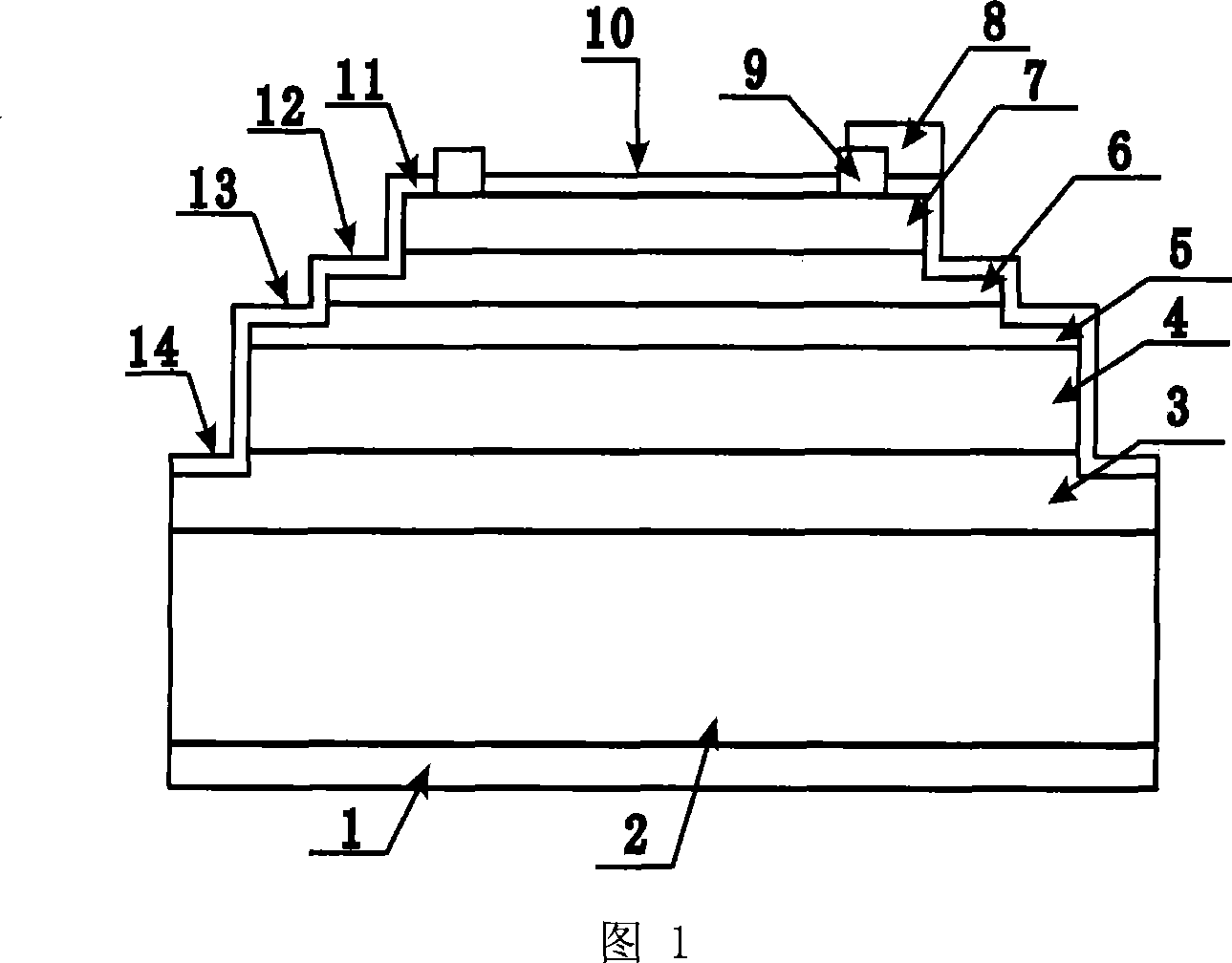
[0030] Referring to Fig. 1, the embodiment structure of the delta-doped 4H-SiC avalanche structure ultraviolet photodetector described in the present invention is: n + Type 4H-SiC substrate 2 and sequential epitaxial growth of heavily doped n + Type buffer layer 3, ultra-lightly doped n -- Type 4 (doping concentration lower than 1.0×10 15 / cm 3 , thickness 2.0 μm), δ-doped n-type layer 5 (doping concentration 3.0×10 17 / cm 3 , thickness 0.125μm), lightly doped n - Type layer 6 (doping concentration 6.0×10 15 / cm 3 , thickness 0.2μm) and heavily doped p + Type layer 7 (doping concentration 5.0×10 18 / cm 3 , with a thickness of 0.3 μm), a device isolation mesa 14, two terminal epitaxial mesas 12 and 13, an oxide layer 11, a p-type contact electrode 9, an n-type contact electrode 1, a pad 8, and a device photosensitive surface 10.

[0031] The example and preparation process of silicon carbide avalanche ultraviolet photodetector are described as follows:

[0032] 1. St...


PUM

PropertyMeasurementUnit
Thicknessaaaaaaaaaa
Doping concentrationaaaaaaaaaa
Thicknessaaaaaaaaaa

Abstract

The invention is concerned with delta-doped 4H-SiC ultraviolet avalanche photodetector and its production, involved with a kind of ultraviolet photodetector. Thedelta-doped 4H-SiC ultraviolet avalanche photodetector and production can enhance the capability of device, eliminate the restrict of quantum yield and respond time to avalanche device, control the thickness of elevated area, the concentration of surface charge and the length of absorbing area. The table-board owns n+ type of 4H-SiC under lay, and there is n+ type buffer layer, super-low-doped n- type layer, delta-doped n type layer, low-doped n- type layer and high-doped p+ type layer on the table-board one by one. The super-low-doped n- type layer, delta-doped n type layer, low-doped n- type layer form active layer. It has at least three table-boards, the lowest one sets on the n+ type buffer layer to isolation of device, the other table-boards set on active layer of device, while the surface of device owns compact Silica passivation film with p type and n type poles.

Description

technical field [0001] The invention relates to an ultraviolet photodetector, in particular to an avalanche structure (APD) ultraviolet photodetector with delta-doped 4H-SiC (silicon carbide) separating an absorption region, a charge region and a multiplication region and a preparation method thereof. Background technique [0002] At present, the detection of ultraviolet light mainly uses silicon-based ultraviolet photodetectors, but since the bandgap width of silicon is 1.1eV, its absorption of light is mainly concentrated in the visible and near-infrared bands, so silicon-based ultraviolet photodetectors require an expensive filtering system. In recent years, the development of the third generation of advanced semiconductor materials represented by SiC has opened up new fields for the research of semiconductor ultraviolet photodetectors. The third-generation advanced semiconductor material has a wide band gap, and the ultraviolet photodetector prepared by it is not sensit...

Claims


Application Information

Patent Timeline
IPC IPC(8): H01L31/107H01L31/18
CPCY02P70/50
Inventor 吴正云朱会丽陈厦平张峰
Owner XIAMEN UNIV
Why Eureka
Try Eureka