Antenna device, array antenna device using the antenna device, module, module array, and package module

An antenna device and feeding antenna technology, applied to antenna arrays, devices that enable antennas to work in different bands at the same time, antennas, etc., can solve the problems of high gain of microstrip antenna unit components not shown, and reduce connection loss Effect

Active Publication Date: 2007-09-05
NIPPON TELEGRAPH & TELEPHONE CORP
View PDF3 Cites 22 Cited by
  • Summary
  • Abstract
  • Description
  • Claims
  • Application Information

AI Technical Summary

Problems solved by technology

[0006] However, in the above-mentioned Patent Document 1, only up to 10dBi is shown as a value for incre

Method used


Image

  • Antenna device, array antenna device using the antenna device, module, module array, and package module
  • Antenna device, array antenna device using the antenna device, module, module array, and package module
  • Antenna device, array antenna device using the antenna device, module, module array, and package module

Examples


no. 1 Embodiment approach

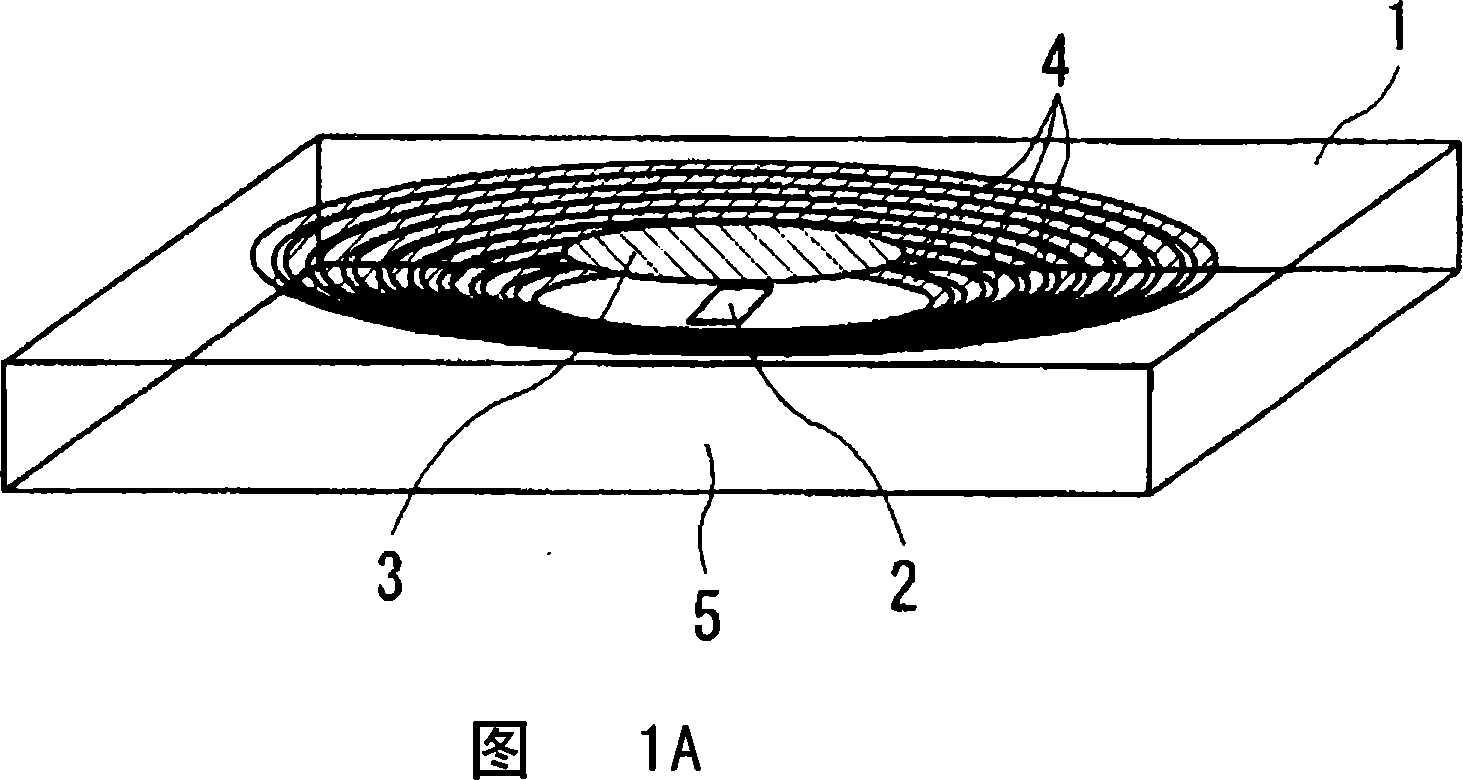
[0104] 1A (perspective view) and FIG. 1B (cross-sectional view) show the configuration of an antenna device according to a first embodiment of the present invention. In these figures, 1 denotes a dielectric substrate, 2 denotes a microstrip antenna, 3 denotes a primary reflector, 4 denotes a secondary reflector, and 5 denotes a floor (ground plane).

[0105] The antenna device of Fig. 1A and Fig. 1B shows following antenna, promptly is made up of the dielectric substrate 1 of 0.1mm by 10 layers every 1 layer, passes the electromagnetic wave that radiates from the microstrip antenna 2 that arranges in the lowest layer on the primary layer that is made of metal plate Reflected by the reflector 3, it is reflected by the secondary reflector 4 made of a circular ring-shaped metal, and operates.

[0106] In the present invention, for example, thinning and miniaturization can be realized by using a high temperature sintered ceramic (HTCC) substrate, and it can be realized with a thic...

no. 2 Embodiment approach

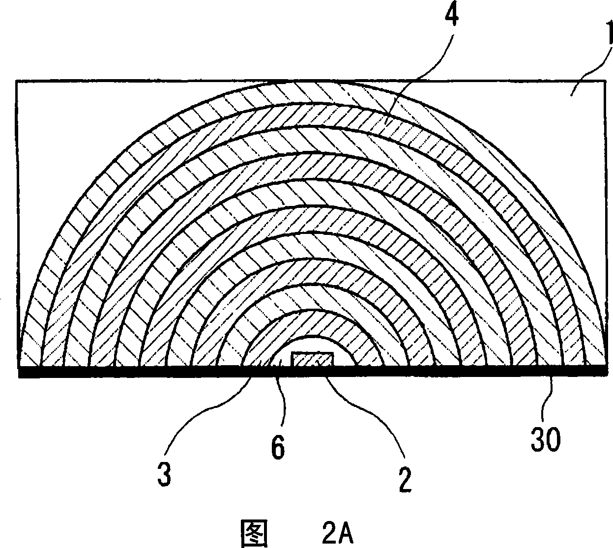
[0110]2A (top view) and FIG. 2B (sectional view) show the structure of an antenna device according to a second embodiment of the present invention. In these figures, 1 denotes a dielectric substrate, 2 denotes a microstrip antenna, 3 denotes a primary reflector, 4 denotes a secondary reflector, 5 denotes a floor, and 6 denotes a slot.

[0111] The structure of the antenna device according to the second embodiment shown in FIGS. 2A and 2B is such that the antenna structure of the antenna device according to the first embodiment is exactly cut in half, and a conductor 30 is disposed at the boundary.

[0112] The secondary reflector 4 can be formed as a circular metal (including an ellipse as mentioned above) or a rectangular ring cut out at an arbitrary angle from the entire circumference.

[0113] According to this configuration, since the mirror image by the conductor 30 is generated as a mirror image antenna, the area can be reduced by approximately half compared with the ant...

no. 3 Embodiment approach

[0117] 3A to 3C show the configuration of an antenna device according to a third embodiment of the present invention. 3A is a perspective view showing the overall structure of the antenna device, FIG. 3B is a cross-sectional view showing FIG. 3A , and FIG. 3C is a diagram showing the definition of arrangement of circular rings. In each of Fig. 3A-Fig. 3C, 1 represents the dielectric substrate, 2 represents the microstrip antenna, 3 represents the primary reflector, 4 represents the secondary reflector, 5 represents the floor, 6 represents the slot, and 7 represents the reradiation from the micro Passive element with electromagnetic waves radiated by antenna 2.

[0118] The antenna structure of Fig. 3A-Fig. 3C is in the antenna structure shown in the first embodiment (Fig. 1A and Fig. 1B), by setting the circular (including ellipse) or rectangular (including square or rectangular) in the primary reflector 3 The slit 6 does not reflect a part of the electromagnetic wave radiate...


PUM

PropertyMeasurementUnit
Thicknessaaaaaaaaaa
Radiusaaaaaaaaaa
Radiusaaaaaaaaaa

Abstract

A small antenna device having an increased gain is provided. The antenna device includes a multilayer dielectric substrate composed of a combination of a plurality of dielectric layers, wherein a feeding antenna is provided in a lower layer of the multilayer substrate, a reflective metal plate is provided above the feeding antenna, and circular or rectangular metal loops are arranged so as to be of increasing diameter from lower layers toward upper layers in the plurality of dielectric layers. There is provided a small-size antenna device having a high gain. The antenna device is formed by a multi-layer dielectric substrate combining a plurality of dielectric layers. A feeding antenna is arranged at the lower layer of the multi-layer substrate. A reflection metal plate is arranged above the feeding antenna. Furthermore, disc-shaped or square loop-shaped metal members are arranged with a diameter increasing from the lower layer toward the upper layer.

Description

technical field [0001] The present invention is used to achieve higher gain antennas using chip antennas, etc., and particularly relates to an antenna device that can effectively achieve higher gain when realizing a system package in which an active device and an antenna are integrated. [0002] The present invention claims the priority of Japanese Patent Application No. 2004-260038 filed on September 7, 2004 and Japanese Patent Application No. 2005-178001 filed on June 17, 2005, the contents of which are cited here. Background technique [0003] Heretofore, various structures of high-gain single-element antennas have been proposed. 30A and 30B show a structural example of a microstrip antenna with a metal wall (see Patent Document 1). 30A and 30B are a perspective view and a cross-sectional view showing the structure of a conventional antenna device, respectively. In Fig. 30A and Fig. 30B, 15 is a cylinder, 16 is a microstrip patch (a microstrip patch), 17 is a power supp...

Claims


Application Information

Patent Timeline
IPC IPC(8): H01Q13/02H01Q13/08H01Q15/14H01Q3/46H01Q19/19
CPCH01Q19/195H01Q19/19H01Q19/17H01Q19/185H01Q1/2283H01Q9/0414H01Q1/38H01Q3/36H01L2224/16225H01L2223/6677H01L2924/15321H01Q5/0065H01Q5/0062H01Q21/061H01L2924/1461H01Q5/378H01Q5/385H01L2924/00H01Q15/14H01Q13/08H01Q7/00
Inventor 关智弘西川健二郎本间尚树常川光一
Owner NIPPON TELEGRAPH & TELEPHONE CORP
Why Eureka
Try Eureka