

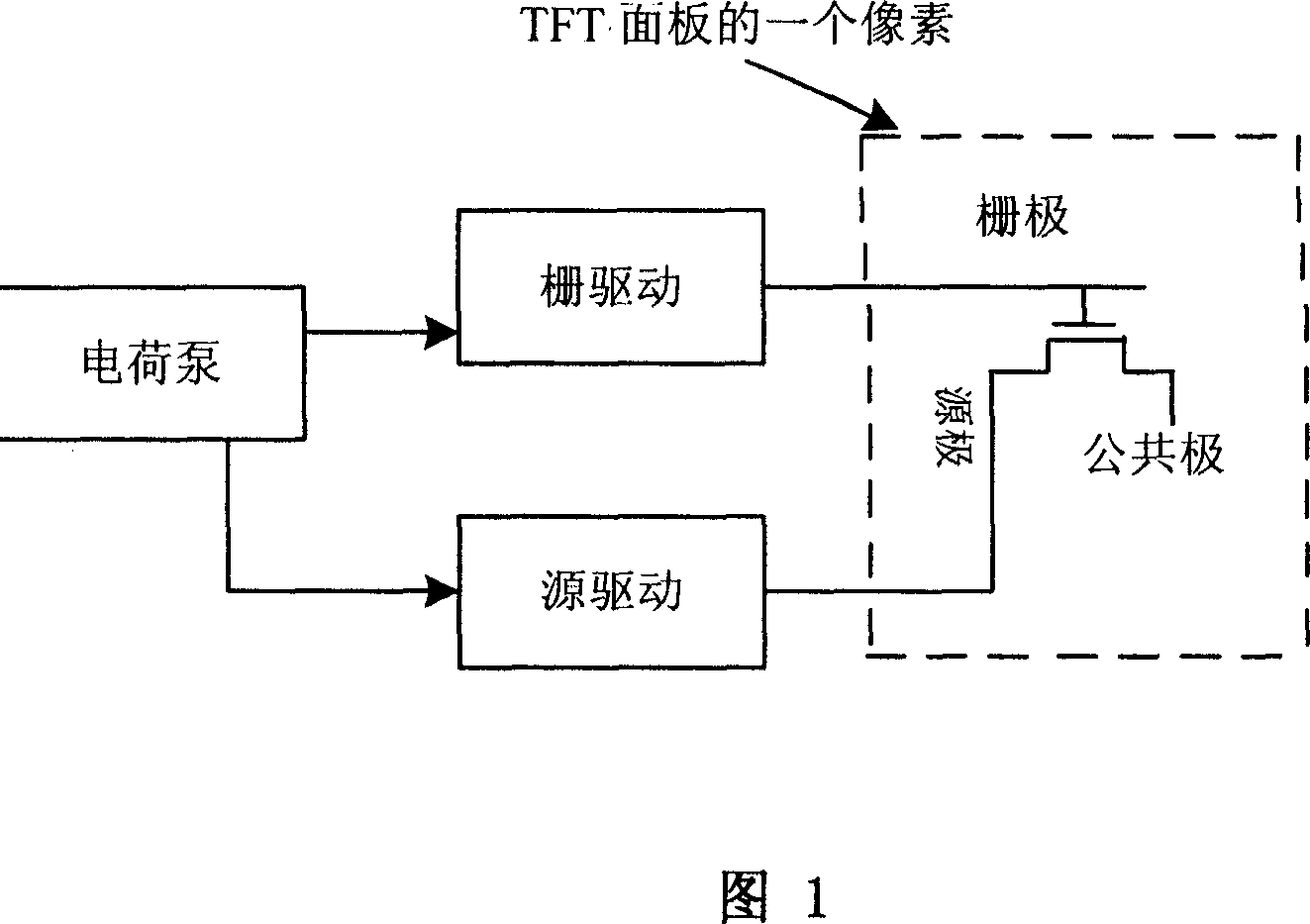
Charge pump circuit in TFT driving circuit
A technology of drive circuit and charge pump, which is applied in the direction of instruments, static indicators, etc., and can solve the problems that are not suitable for low-voltage operation
- Summary
- Abstract
- Description
- Claims
- Application Information
AI Technical Summary
Problems solved by technology
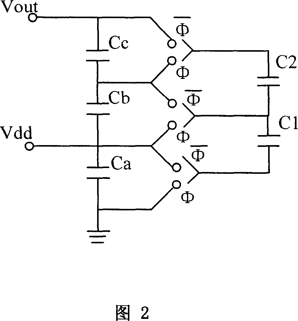
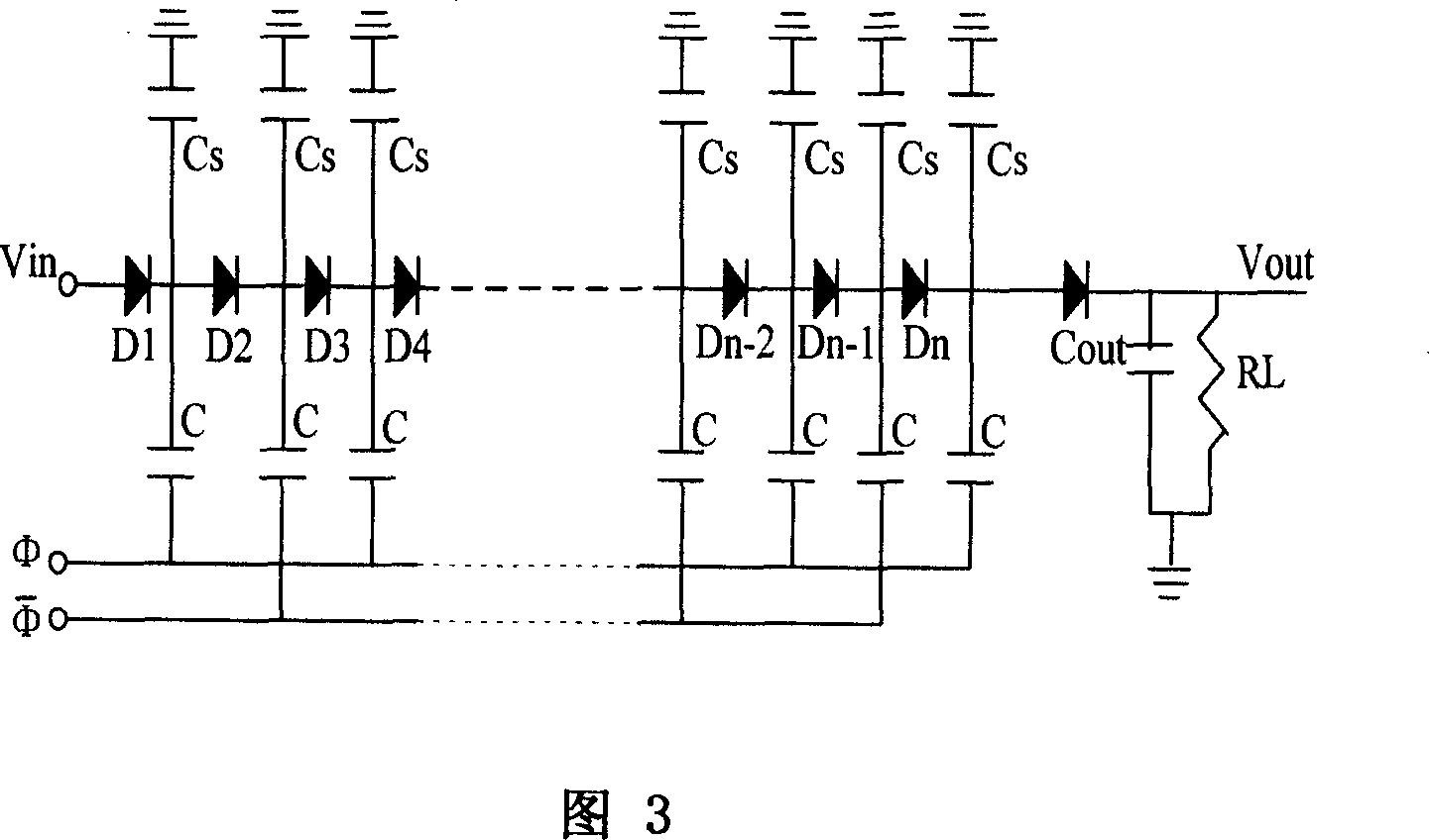
Method used
Image

Examples
Embodiment Construction
[0024] These and other advantages of the present invention will become apparent upon reading the following detailed description of the aspects, including the description of the accompanying drawings. The present invention will be described in detail below in conjunction with the accompanying drawings.
[0025] Figure 4 is a functional block diagram of a digitally controlled charge pump, which consists of a control logic and many separate analog blocks with different functions. The various modules can be divided according to their independent functions. VDD provides the reference voltage of the charge pump and is directly input into the positive doubler 41 and the negative doubler 45 . The output terminal of the logic control circuit is sequentially connected in parallel with a positive doubler 41, a positive quadruple 42, a positive sixfold 43, a positive voltage output stage 44, a negative doubler 45, a negative tripler 46, and a negative tripler 45. Five voltage multiplier...
PUM
 Abstract
Description
Claims
Application Information