Ceramic powder, dielectric paste using same, multilayer ceramic electronic component, and method for production thereof

A ceramic powder and electronic component technology, which is applied in the field of ceramic powder, can solve the problems of poor manufacturing yield, cracks, peeling, etc., and achieve the effects of improving manufacturing yield, reducing cracks or delamination, and improving withstand voltage

Inactive Publication Date: 2007-09-12
TDK CORPARATION
View PDF1 Cites 1 Cited by
  • Summary
  • Abstract
  • Description
  • Claims
  • Application Information

AI Technical Summary

Problems solved by technology

[0005] However, when the internal electrode layer is formed using the conductive paste for internal electrodes mainly composed of base metals such as Ni, for example, the thickness of the dielectric ceramic layer is set to be 10 μm or less, or the number of stacked layers is 100 or more, the internal electrode layer may The shrinkage and expansion of the dielectric ceramic layer are different from the shrinkage behavior of the dielectric ceramic layer, resulting in possible peeling (delamination) or cracks, resulting in a problem of poor manufacturing yield

Method used


Image

  • Ceramic powder, dielectric paste using same, multilayer ceramic electronic component, and method for production thereof
  • Ceramic powder, dielectric paste using same, multilayer ceramic electronic component, and method for production thereof
  • Ceramic powder, dielectric paste using same, multilayer ceramic electronic component, and method for production thereof

Examples


Embodiment approach

[0031] Hereinafter, the ceramic powder and dielectric paste of the present invention are applied, and further, a laminated ceramic electronic component (here, a laminated ceramic capacitor) using them and a method of manufacturing the same will be described in detail.

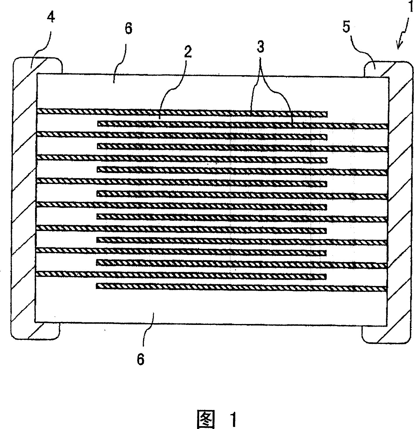
[0032] First, a multilayer ceramic capacitor using the ceramic powder of the present invention will be described. As shown in FIG. 1 , in a multilayer ceramic capacitor 1 , a plurality of dielectric ceramic layers 2 and internal electrode layers 3 are alternately stacked to form a device body. The internal electrode layers 3 are laminated so that the opposite end faces of the device body are exposed alternately, and a pair of external electrodes 4, 5 are formed on both ends of the device body to conduct with these internal electrode layers 3 . In addition, in the device body, the outer dielectric layer 6 is arranged at both ends of the stacking direction of the dielectric ceramic layer 2 and the internal electro...

Embodiment

[0063] Hereinafter, specific examples to which the present invention is applied will be described based on experimental results.


PUM

PropertyMeasurementUnit
specific surface areaaaaaaaaaaa
thicknessaaaaaaaaaa
thicknessaaaaaaaaaa

Abstract

As the ceramic powder fated to form dielectric ceramic layers in a multilayer ceramic electronic component resulting from alternately stacking the dielectric ceramic layers and internal electrode layers, a ceramic powder that possesses a perovskite-type crystal structure and satisfies an expression X < 3, wherein X denotes the weight ratio Wt / Wc of the tetragonal phase content Wt and the cubic phase content Wc, is used. The weight ratio Wt / Wc of the tetragonal phase and the cubic phase is determined by the polyphasic analysis in accordance with the Rietveld method. The ceramic powder is a barium titanate powder, for example. The specific surface area of the ceramic powder is in the range of 4 to 10 m 2 / g.

Description

technical field [0001] The present invention relates to a ceramic powder used for forming a dielectric ceramic layer in a laminated ceramic electronic component in which dielectric ceramic layers and internal electrode layers are alternately laminated, and particularly to a ceramic powder useful for improving the withstand voltage characteristics of a laminated ceramic electronic component. Furthermore, it is related with the dielectric paste which used the said ceramic powder, a laminated ceramic electronic component, and its manufacturing method. Background technique [0002] For example, multilayer ceramic capacitors, one of the multilayer ceramic electronic components, have a structure in which a plurality of dielectric ceramic layers and internal electrode layers are alternately stacked, and are widely used as small, large-capacity, and high-reliability electronic components. There are also many cases where multiple multilayer ceramic capacitors are used in one electron...

Claims


Application Information

Patent Timeline
Patent Type & Authority Applications(China)
IPC IPC(8): H01B3/12H01G4/12H01G4/30C04B35/46
CPCC04B2235/5409C04B2235/5445H01G4/30C04B35/4682H01G4/1209C04B2235/765H01G4/1227C04B2235/663C04B2235/6567C04B2235/6025C04B2235/6582C04B35/638C04B2235/6562C04B2235/6584C04B2235/762C04B2235/6588C04B35/46C04B35/468C04B2111/90
Inventor 原治也渡边康夫佐藤阳
Owner TDK CORPARATION
Why Eureka
Try Eureka