Static protection circuit suitable for radio frequency identification label chip
A technology for radio frequency identification tags and electrostatic protection, which is applied in the field of passive RFID tag chips, can solve the problems of low efficiency, high power consumption, and inability to share current equally, so as to reduce area, reduce power consumption, and improve ESD The effect of protective performance
- Summary
- Abstract
- Description
- Claims
- Application Information
AI Technical Summary
Problems solved by technology
Method used
Image
Examples
example
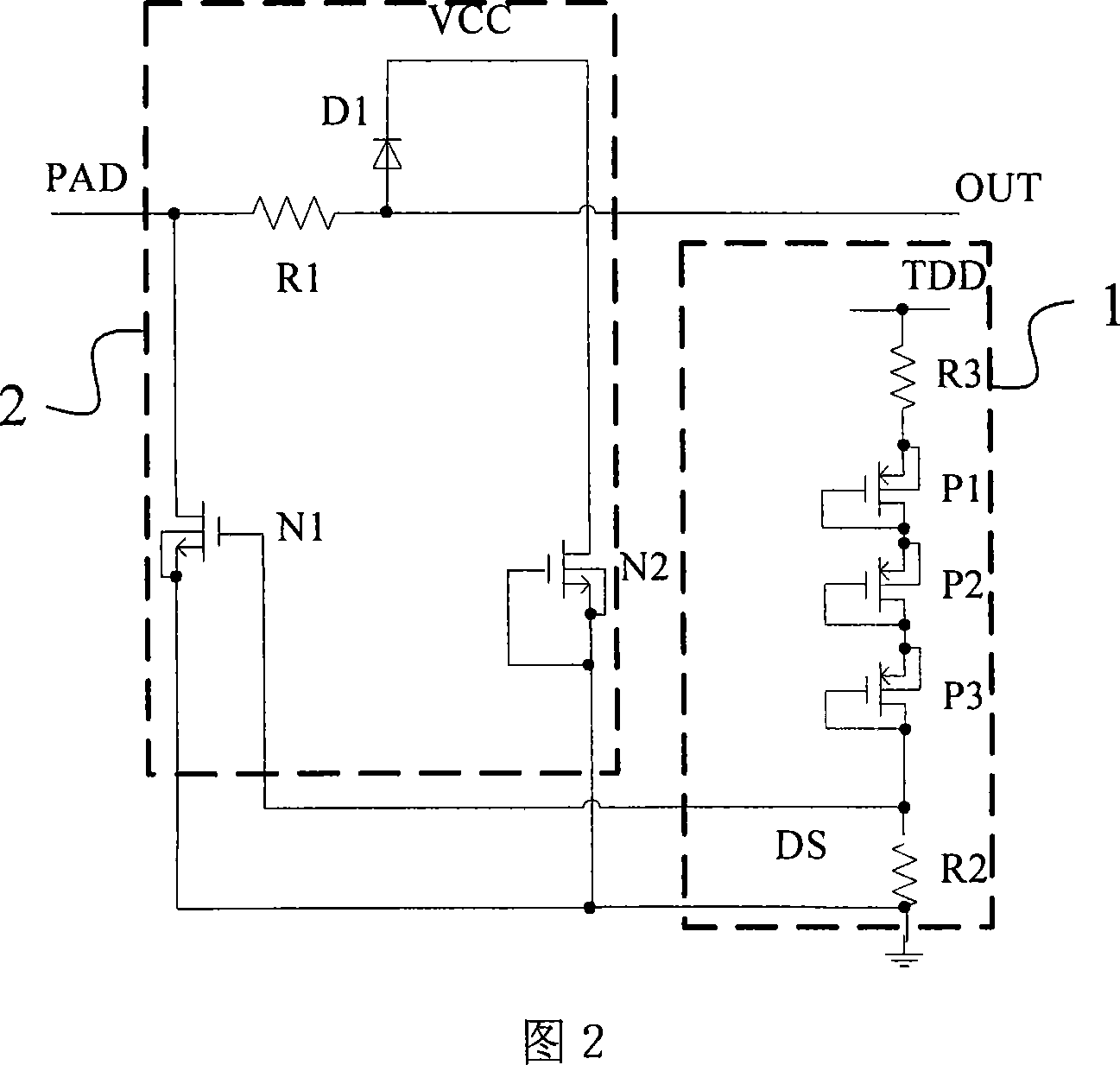
[0022] The description of this example is based on the circuit design based on the SMIC (SMIC) 0.35μm process with embedded EEPROM. The process library defines the threshold voltage of the PMOS transistor as V THP =0.7V, the threshold voltage of the NMOS tube is V THN =0.7V, R3 resistance is 10KΩ. The withstand voltage of an ordinary NMOS tube is 9.8V.
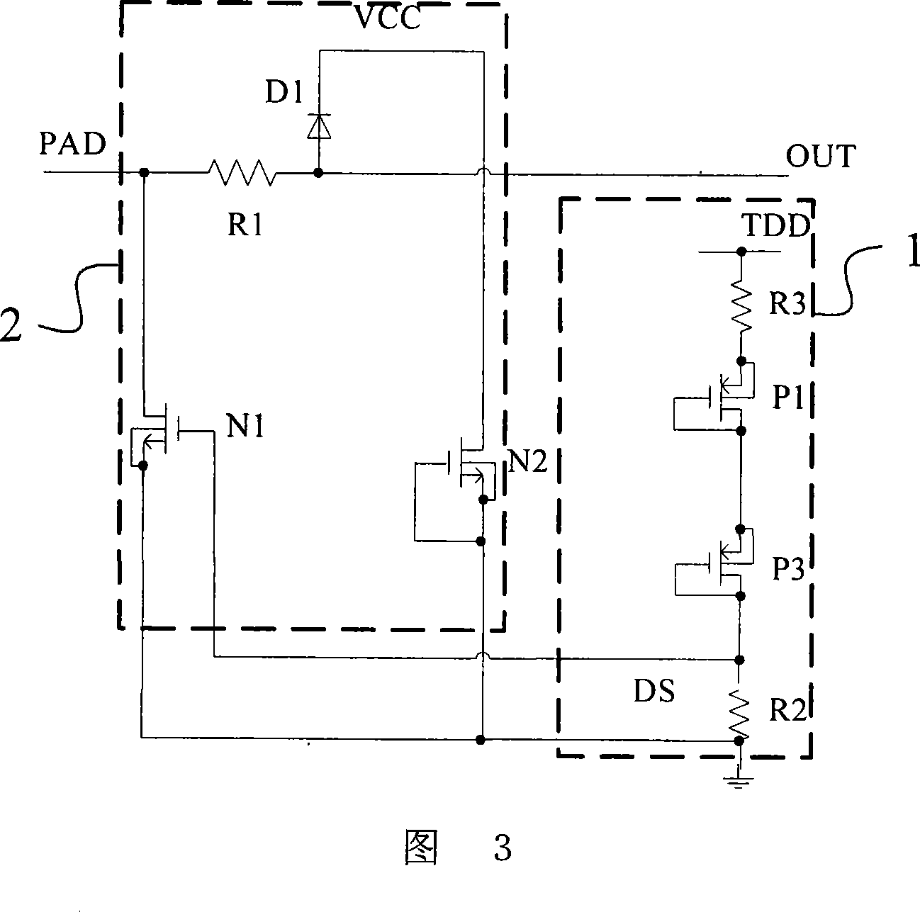
[0023] circuit operation, if V TDD > 4.8V, the circuit enters b high voltage discharge state, if V TDD <4.8V, the circuit enters a normal state. When an electrostatic pulse appears on the input node PAD, the circuit directly enters the c electrostatic discharge state. In any case, the maximum voltage of the output node OUT is 9.3V, so it will not cause damage to the circuit device.
[0024] In actual production, the NMOS tubes N1 and N2 will adopt an ESD protection tube structure to increase the size of the source and enhance the heat dissipation capability.
PUM
 Abstract
Description
Claims
Application Information


