

Leadless integrated circuit protection device
A technology for circuit protection and protection components, which is applied in the field of leadless integrated circuit protection components to achieve the effects of good performance characteristics, low impedance and low conductance
- Summary
- Abstract
- Description
- Claims
- Application Information
AI Technical Summary
Problems solved by technology
Method used
Image

Examples
Embodiment Construction
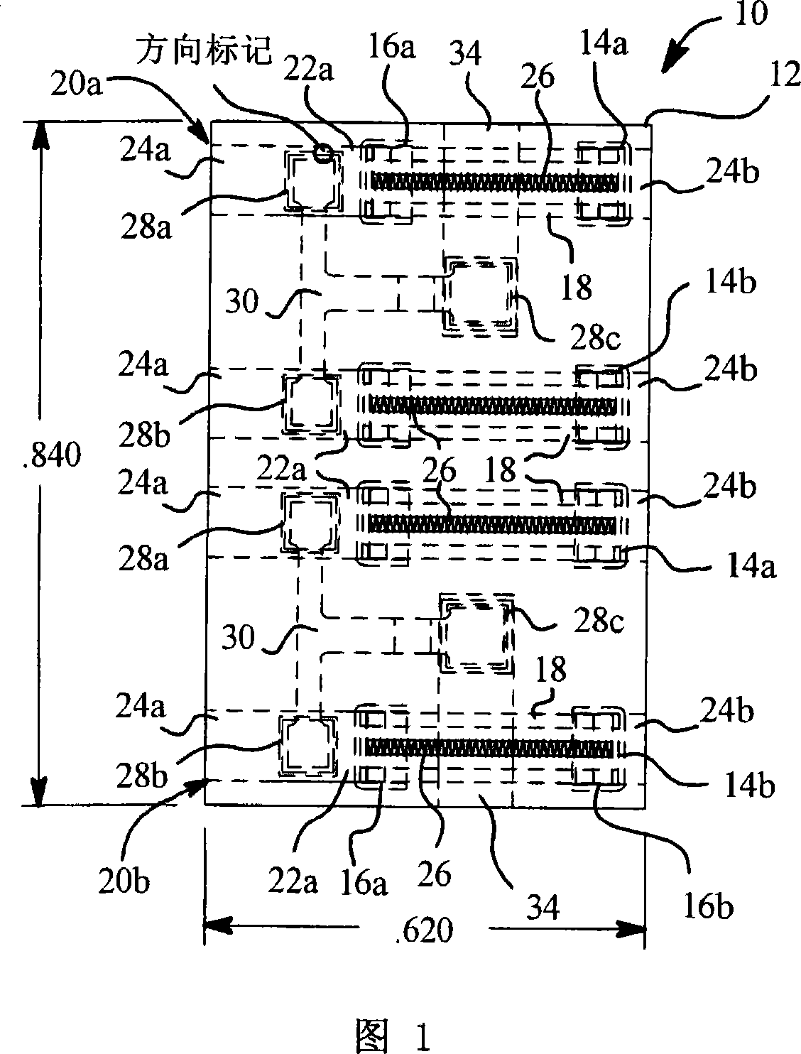
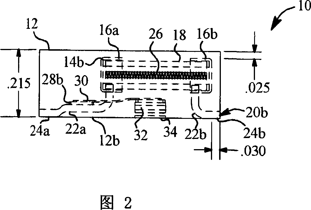
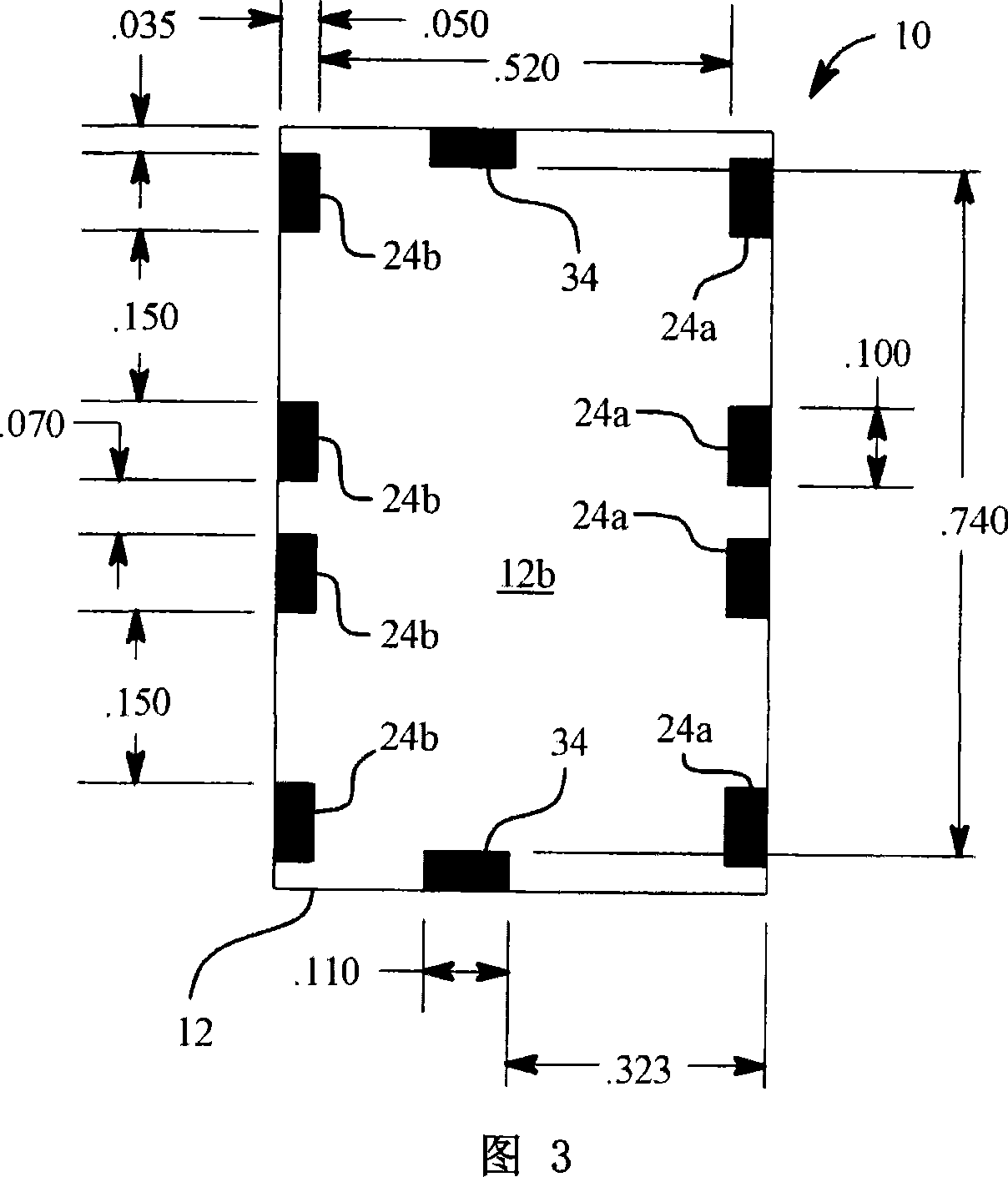
[0052] Detailed herein are embodiments of leadless circuit protection components that meet the current goals of the semiconductor industry to use components that are smaller and can be produced at a faster rate. Embodiments disclosed herein are compliant with semiconductor industry standards such as those set forth in JEDEC 95 Edition, Design Guide 4.19, Interleaved Quad No-Leads, and In-Line Multi-Nine Packages (“QFN”).
[0053] The components in the embodiments are lead frame based and encapsulated in a low impedance, conductance, capacitance ("RLC") package plastic. Lead frame construction designs the type, characteristics and configuration of the circuit protection components packaged in the component for the specific application. components have good heat dissipation capabilities. The integration of overcurrent and overvoltage functions helps ensure proper coordination, and close proximity of circuit protection components packaged throughout the unit enhances electrical ...
PUM
 Abstract
Description
Claims
Application Information