Wafer level packaging method and its structure

A chip packaging and chip technology, which is applied in the field of integrated wafer-level packaging technology, can solve the problems of increasing packaging structure failures and complex processes, and achieve the effects of reducing time and complexity, reducing packaging time, and being easy to rework.

Inactive Publication Date: 2007-11-14
中国台湾格雷蒙股份有限公司
View PDF3 Cites 6 Cited by
  • Summary
  • Abstract
  • Description
  • Claims
  • Application Information

AI Technical Summary

Problems solved by technology

[0005] On the other hand, in order to reduce the size of the electronic system, reduce the signal loss and noise caused by the connection of the components in the circuit board through the external wire connection, and reduce the failure probability caused by the bad connection wires, a semiconductor manufacturing process has also been developed. In this way, the integrated process of integrating passive components in the semiconductor packaging structure, but it often needs to add additional processes to form passive components, not only the process is complicated, but also the failure of the packaging structure is increased.

Method used


Image

  • Wafer level packaging method and its structure
  • Wafer level packaging method and its structure
  • Wafer level packaging method and its structure

Examples


Embodiment Construction

[0093] The purpose, functions and advantages of the present invention can be better understood through the following detailed description and corresponding illustrations.

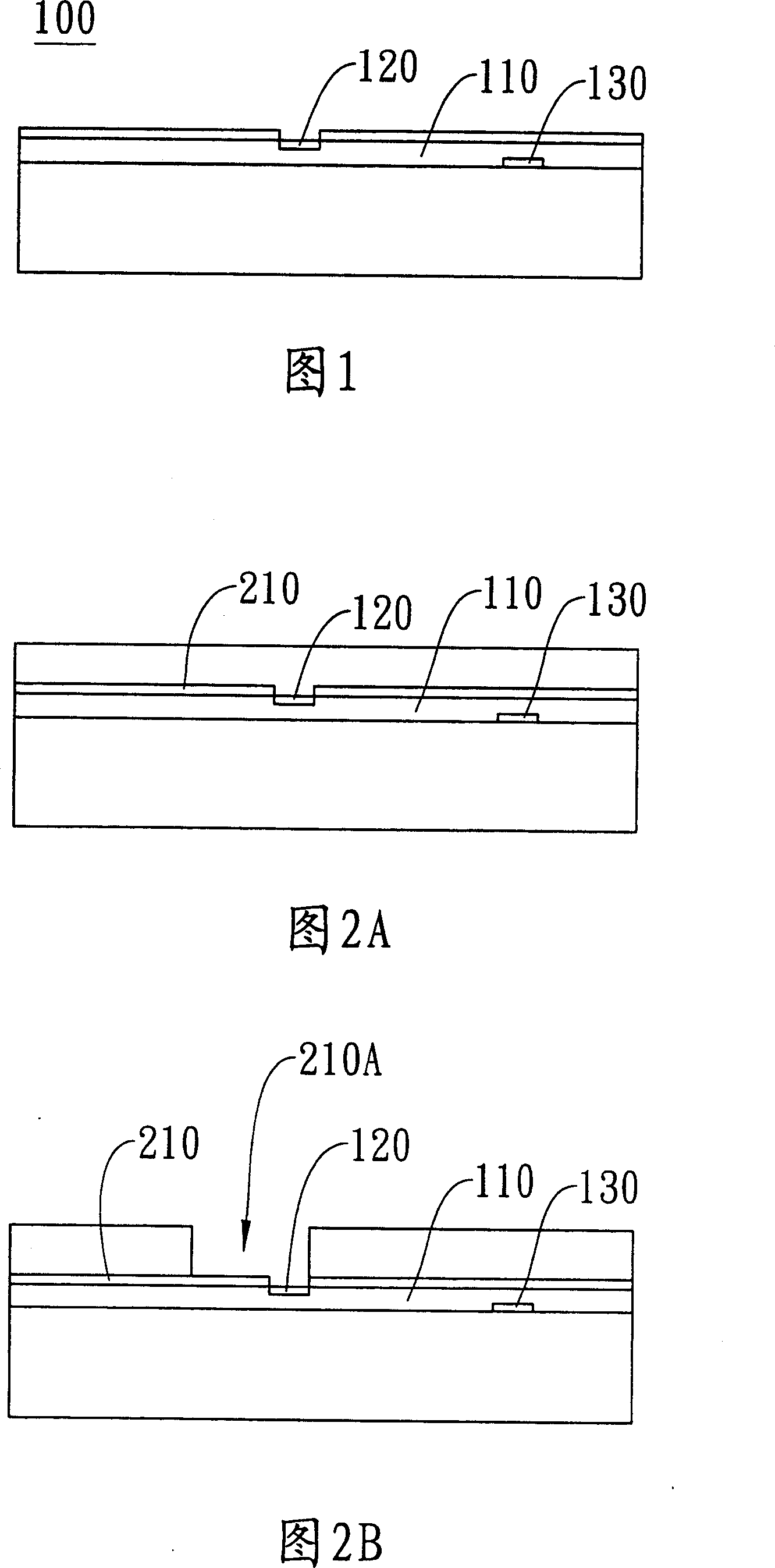
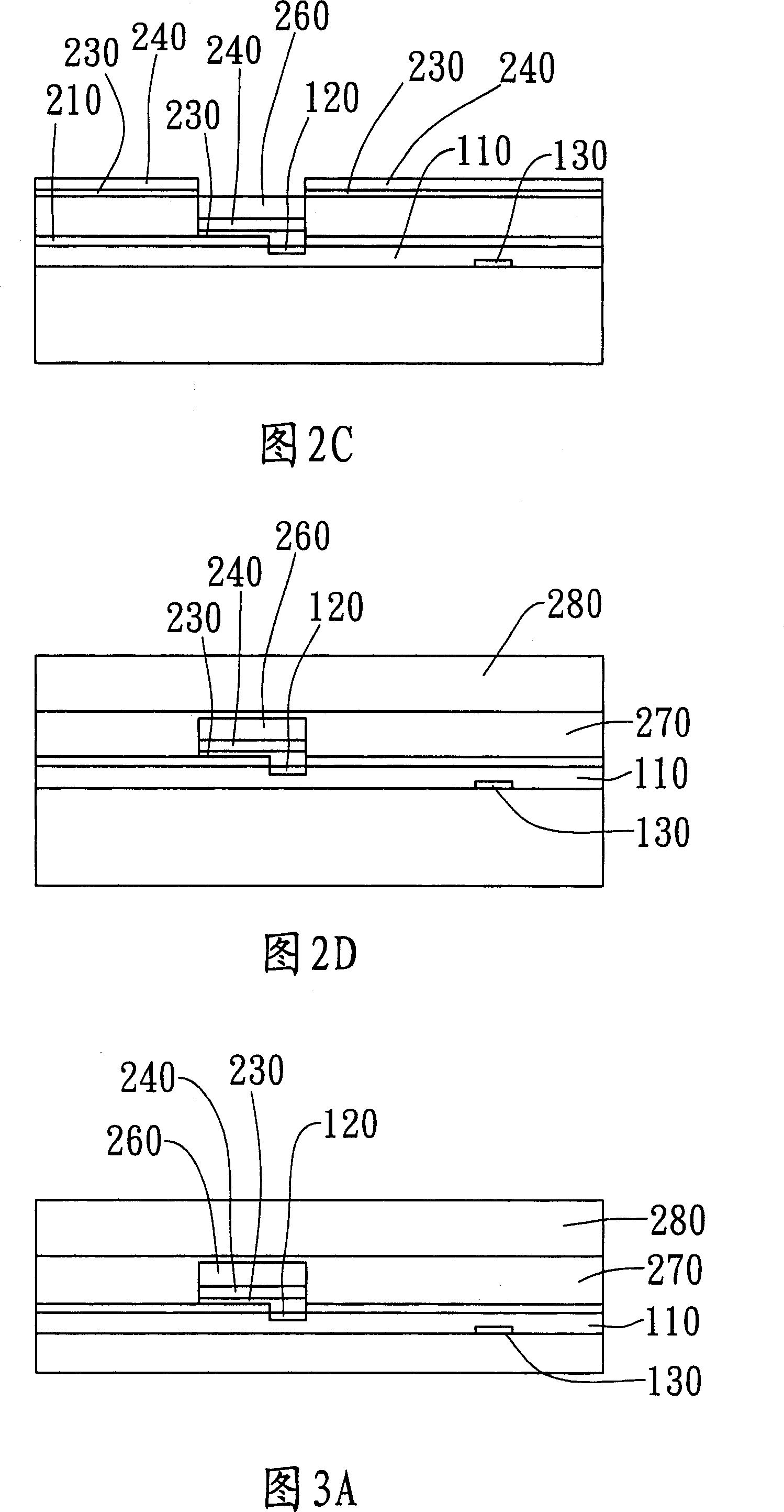
[0094] Please refer to FIG. 1, which is a chip 100 according to a preferred embodiment of the present invention, the chip 100 includes at least one circuit element 110, at least one surface connection pad 120 and at least one internal connection pad 130, and the circuit element 110 is located on the In the chip 100 , the surface connection pad 120 is located on the surface side of the chip 100 , and the internal connection pad 130 is located in the chip 100 and is electrically connected to the circuit element 110 .

[0095] First, a surface activation process can be selectively implemented according to needs. The surface activation process is used to remove pollutants on the wafer surface and surface connection pads, such as oxides or particles, so as to increase the connection between the wafer surface and ...


PUM


Abstract

The invention is an integrated wafer packaging structure, comprising a chip, at least a passive component, an interface layer, an insulating layer, at least a connection, an internal connecting pad and a protection layer, where the chip comprises a surface connecting pad, an internal connecting pad and a circuit component, the passive component is formed on one side of the chip, the interface layer increases the bond between the passive component and the chip, the insulating layer covers part of the surface on the other side of the chip, the connection covers part of the surface of the insulating layer and the internal connecting pad and is used to connect with the internal connecting pad, and the protection layer is used to protect the chip.

Description

technical field [0001] The present invention relates to an integrated packaging process method, especially an integrated chip-level packaging process method, which can form at least one passive element in the packaging structure to effectively reduce the packaging volume and system volume and reduce the external contact with the passive element. Signal attenuation and failure problems caused by connections. Background technique [0002] The packaging methods of integrated circuits have been developed for a long time, and can be roughly divided into two types: pin insertion and surface mount. The surface mount method completes the electrical connection with the substrate through the metal pad. [0003] In the development process of the surface mount method, with the increasing degree of integration of the substrate circuit, many packaging methods have been developed, such as chip-scale packaging (chipscale package, CSP) with a ratio of bare die to package body area of ​​less...

Claims


Application Information

Patent Timeline
Patent Type & Authority Applications(China)
IPC IPC(8): H01L21/60H01L25/00H01L23/488
CPCH01L2924/0002
Inventor 杨辰雄
Owner 中国台湾格雷蒙股份有限公司
Why Eureka
Try Eureka