Slow light controlled photon crystal coupled switch

A technology of photonic crystal and coupling switch, which is applied in the coupling of optical waveguide, optical waveguide light guide, optics, etc., can solve the problems of technical public reporting, etc., and achieve the effects of short coupling length, improved integration, and small volume

Inactive Publication Date: 2007-11-28
SHANGHAI JIAO TONG UNIV
View PDF0 Cites 8 Cited by
  • Summary
  • Abstract
  • Description
  • Claims
  • Application Information

AI Technical Summary

Problems solved by technology

At present, there is no relevant technical public report at home and abroad

Method used


Image

  • Slow light controlled photon crystal coupled switch
  • Slow light controlled photon crystal coupled switch
  • Slow light controlled photon crystal coupled switch

Examples


Embodiment

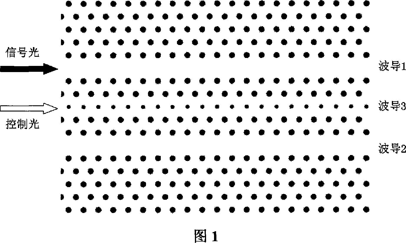
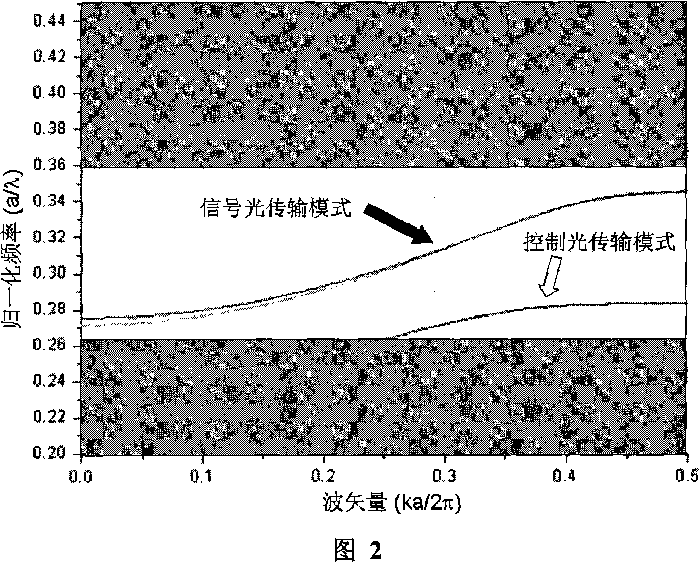
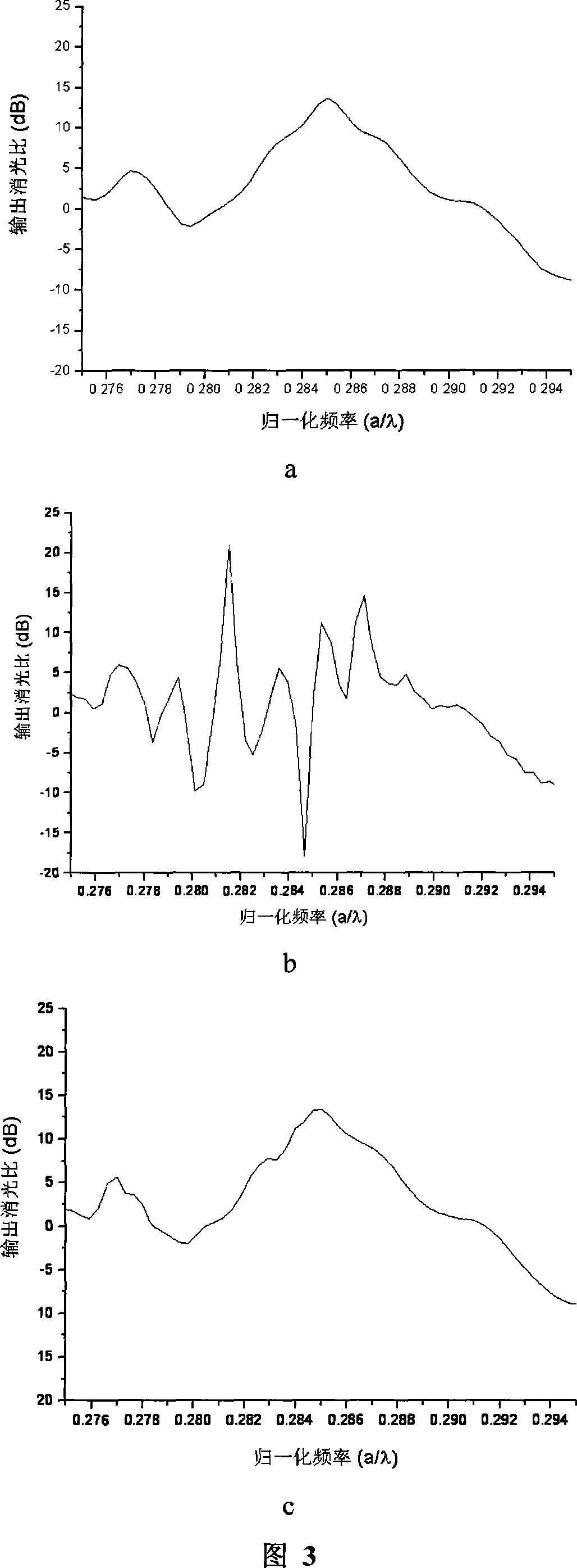
[0021] The composition of the photonic crystal material is to add dielectric rods with high dielectric constant (ε=12) to the background material of low dielectric rate (ε=2.1). The dielectric rods are arranged in a hexagonal lattice, and the lattice constant is a. The radius of the rod is 0.2a. Two line-defect waveguides, labeled waveguides 1 and 2, are realized by removing two rows of dielectric rods. In addition to having the same dielectric constant as the background material, the material of the waveguide also has the Kerr nonlinear effect, and the Kerr coefficient is 3.25×10 -9 cm 2 / W. The line defect waveguides are separated by 5 rows of dielectric rods. A row of dielectric rods located at the center of the 5 rows of dielectric rods has a radius of 0.14a, which acts as a line defect waveguide for controlling the passage of light, and is marked as waveguide 3. The entire structure has a length of 20a. The present invention first requires obtaining the photonic band...


PUM


Abstract

The invention discloses a photon transistor coupling switch controlled by slow light, which is characterized by the following: adding dielectric bar with different dielectric constants as the background material into the background material; arranging the dielectric bar at square lattice or hexagonal lattice; removing two rows of dielectric rod to realize defective waveguide of signal transmitting wire with two non-linear Kerr effect; separating two defective waveguides of signal transmitting wire by odd rows of dielectric bar; changing the radius of one row of dielectric bar in the center of the odd rows of dielectric bar to control the defective waveguide; selecting optical signal with minimum group speed to pass the defective waveguide as slow light control light; inputting the slow light control light through controlling the defective waveguide; changing the strike of signal light of certain defective waveguide of signal transmitting wire into another defective waveguide of signal transmitting wire to output; using shorter coupling length to change the coupling switch condition dynamically; improving the integrated degree of integrated light path and reducing the operational power.

Description

technical field [0001] The invention relates to a photonic crystal coupling switch, in particular to a nonlinear material photonic crystal coupling switch controlled by slow light, which is suitable for optical communication systems and integrated optical circuits. Background technique [0002] The integrated optical circuit will be the main device of the next-generation optical communication system, which has the advantages of low cost, small size, and easy mass production. As the most potential materials for the realization of integrated optical circuits, photonic crystals have been widely valued. Photonic crystals are composed of periodically arranged dielectric materials that prohibit the passage of light in certain frequency ranges, a phenomenon known as the photonic bandgap. Using this characteristic, by causing certain defects in the material, the transmission of optical signals can be realized. Photonic crystal coupling switch is one of the key components of integr...

Claims


Application Information

Patent Timeline
Patent Type & Authority Applications(China)
IPC IPC(8): G02F1/35G02B6/12G02B6/26
Inventor 曲扬姜淳
Owner SHANGHAI JIAO TONG UNIV
Why Eureka
Try Eureka