

A clock adjustment algorithm based on minimum two multiplexing model
A least square method and clock adjustment technology, applied in the field of communication, can solve the problems of complex implementation, high cost, and high cost, and achieve the effect of ensuring accuracy
- Summary
- Abstract
- Description
- Claims
- Application Information
AI Technical Summary
Problems solved by technology
Method used
Image

Examples
Embodiment
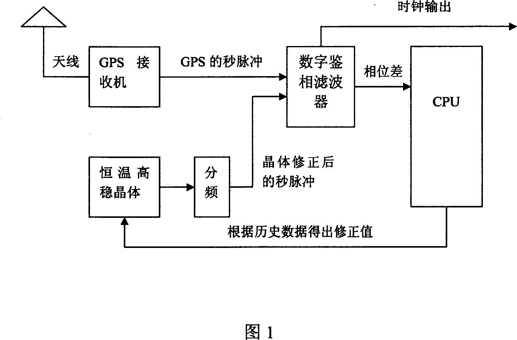
[0033] As shown in Figure 1, it is a schematic structural diagram of a clock synchronization device. The clock synchronization device is composed of a digital phase detector filter, a GPS receiver, a CPU and a constant temperature high-stable crystal. The digital phase detector filter is connected with the GPS receiver, and the digital phase detector The phase detection filter is connected with the CPU and the constant temperature high stability crystal to form a circuit. CPU: Rabbit2000, the performance is about the same as the 8051 series with 16M crystal oscillator.
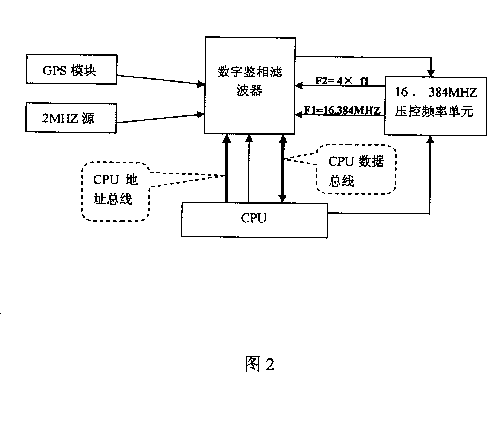
[0034] As shown in Figure 2, it is a structural schematic block diagram of a digital phase detection filter, and the present invention aims at the 1pps second pulse signal (or equivalent 1pps signal) provided by this low-cost GPS receiving module as an external reference comparison signal source , use the equivalent 1pps signal output of the local voltage-controlled quartz crystal oscillator controlled by the d...
PUM
 Abstract
Description
Claims
Application Information