Cutting method for wafer

A cutting method and wafer technology, applied to fine working devices, stone processing equipment, manufacturing tools, etc., can solve the problems of high price, insufficient cleaning effect, and decline in the quality of semiconductor chips, and achieve the effect of inhibiting corrosion and maintaining the cleaning effect

Inactive Publication Date: 2007-12-12
DISCO CORP
View PDF1 Cites 4 Cited by
  • Summary
  • Abstract
  • Description
  • Claims
  • Application Information

AI Technical Summary

Problems solved by technology

[0005] However, there is a problem that the activated cutting water mixed with carbon dioxide has a strong acidity, and it corrodes the bonding pads formed on the surface of the semiconductor chip, especially the bonding pads mainly formed of aluminum, resulting in the ionization of aluminum and the occurrence of solder defects. Corrosion (leaching out) of pad leaching (液け出す), which degrades the quality of semiconductor chips
[0006] On the other hand, in the case where the concentration of carbon dioxide i

Method used


Image

  • Cutting method for wafer
  • Cutting method for wafer
  • Cutting method for wafer

Examples


Embodiment Construction

[0021] Hereinafter, a wafer cutting method as the best mode for carrying out the present invention will be described with reference to the drawings.

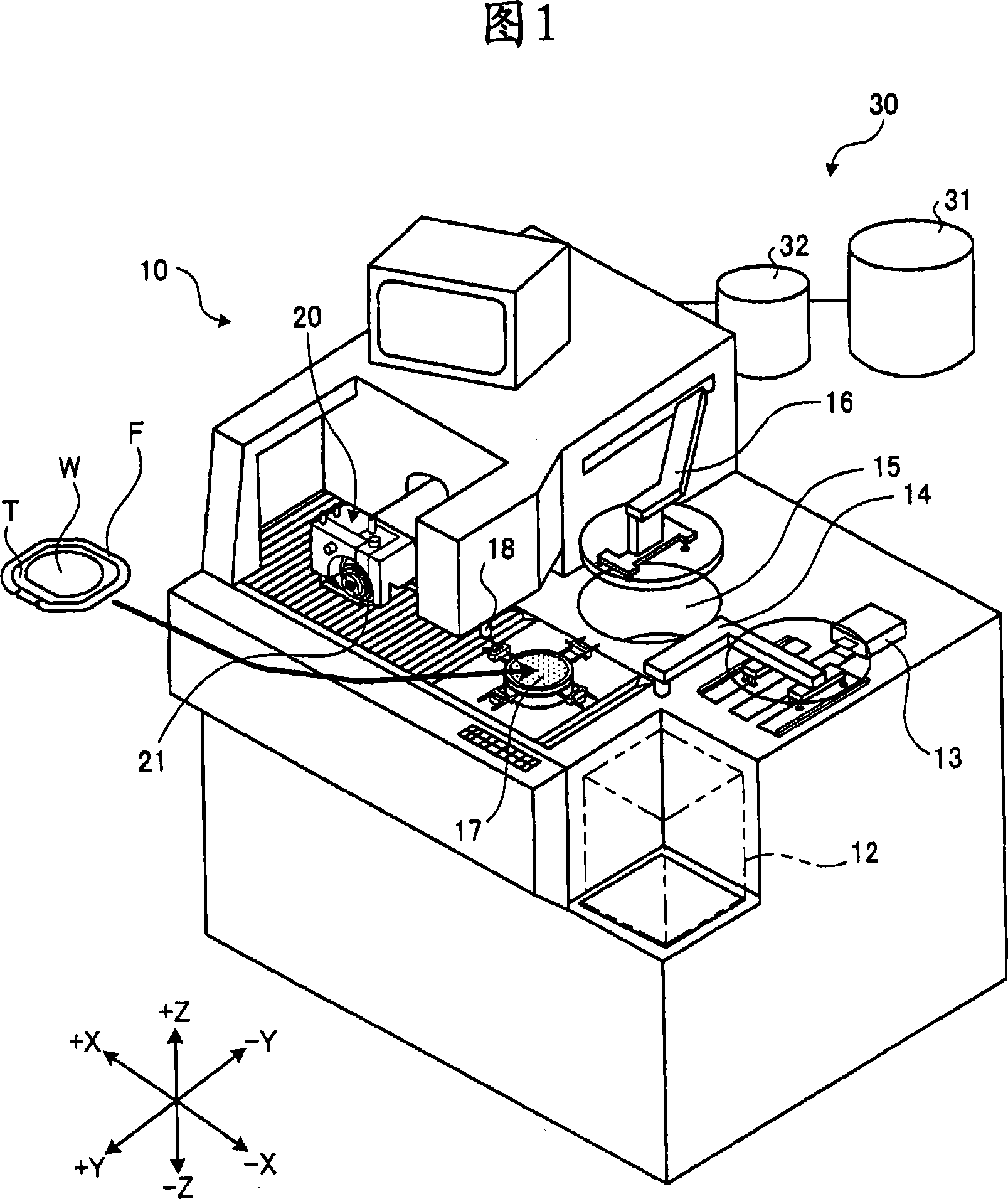
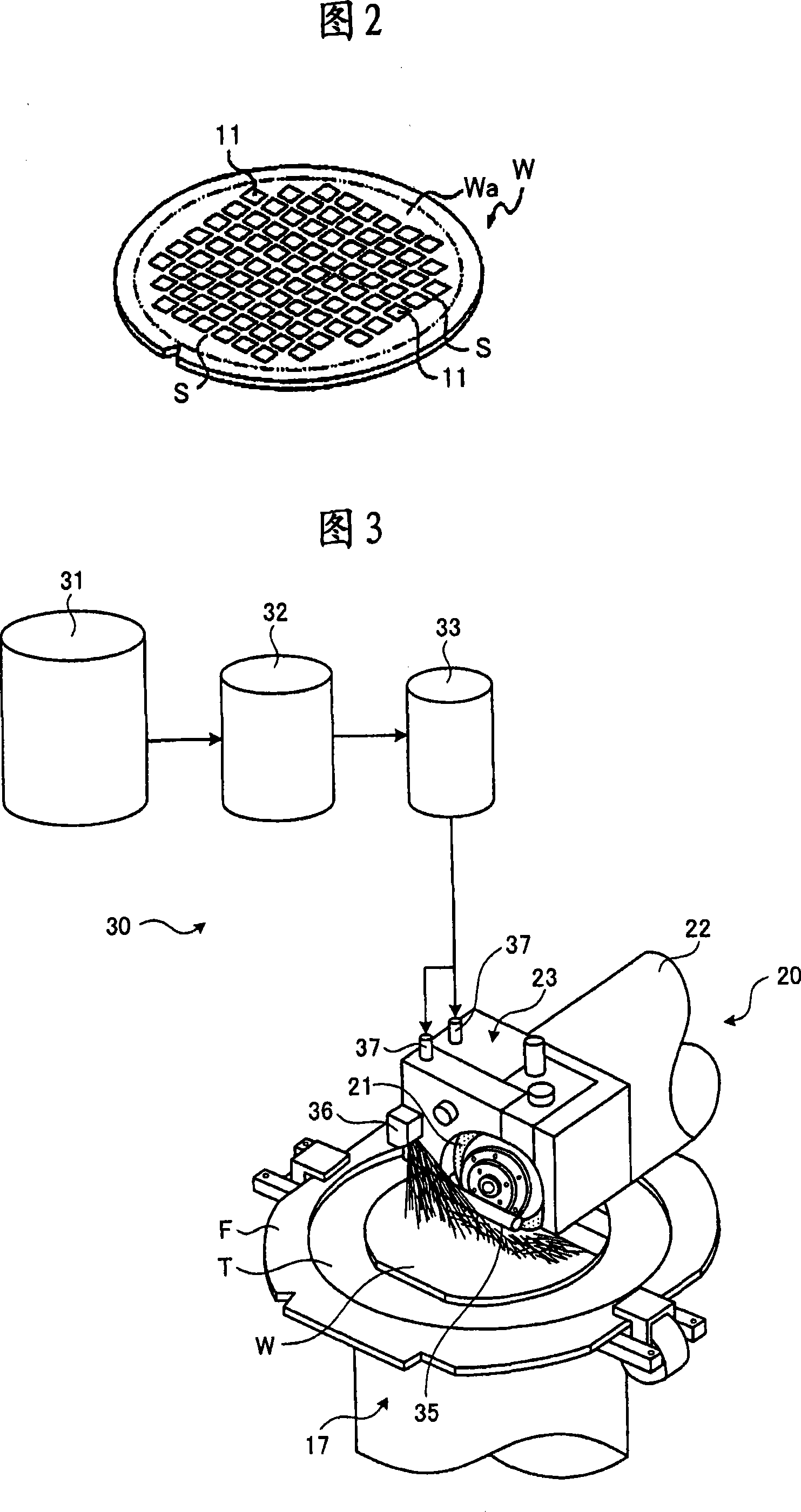
[0022] 1 is a schematic perspective view showing a configuration example of a cutting apparatus for carrying out a wafer cutting method according to an embodiment of the present invention, FIG. 2 is a perspective view showing a configuration example of a wafer applied to this embodiment, and FIG. A perspective view of a configuration example of a cutting water supply device. The cutting device 10 has a transport device 13, a transport device 14, a cleaning device 15, and a transport device 16. At the same time, it has a chuck table 17 integrally formed with the frame F to hold the wafer W, a camera 18 for alignment, and a chip holder for cutting. A cutting device 20 for wafer W on chuck table 17 and a cutting water supply device 30 for supplying cutting water to wafer W are provided.

[0023] First, the wafer W is pasted on the...


PUM


Abstract

The invention provides a cutting process of wafer. The said process can cheaply and simply keep cleaning effect without corroding the welding pad containing aluminium and divide the wafer into a number of semiconductor chips. In the said cutting process, cold machining water of below 15 degree mixed with carbon dioxide is supplied to wafer W through chemistry reaction with an eye to one reason of welding pad corroding, at the same time the cutting process of wafer W is performed using cutting tool (21), in order to slow the reaction rate of digesting of aluminium and prevent the welding pad from corrode.

Description

technical field [0001] The present invention relates to a wafer cutting method for dividing a wafer having bonding pads formed on its surface into individual semiconductor chips. Background technique [0002] A plurality of semiconductor wafers formed by dividing semiconductor chips such as ICs, LSIs, and CCDs at chip intervals are divided into individual semiconductor chips by a cutting device having a cutting tool. [0003] Here, since the cutting blade cuts into the wafer while rotating at a high speed during chip spacing cutting, cutting water is sprayed onto the contact portion to cool the contact portion between the wafer and the cutting blade. Moreover, the cutting water can prevent the cutting chips generated by cutting from adhering to the wafer, and at the same time, it can also play the role of removing the attached cutting chips and cleaning the surface of the wafer. If pure water is used as such cutting water, the specific resistance value will increase and sta...

Claims


Application Information

Patent Timeline
IPC IPC(8): B28D5/00
Inventor L・L・森寺本政由志押领司礼奈
Owner DISCO CORP
Why Eureka
Try Eureka