Semiconductor device, unique ID of semiconductor device and method for verifying unique ID

A semiconductor, the only technology, applied in the direction of semiconductor devices, semiconductor/solid-state device components, computer security devices, etc., can solve the problems of complex initial value setting, troublesome retesting, and troublesome preparation, so as to reduce the number of laser trimming and improve Difficulty, the effect of shortening the manufacturing time

Inactive Publication Date: 2007-12-12
RENESAS TECH CORP
View PDF1 Cites 5 Cited by
  • Summary
  • Abstract
  • Description
  • Claims
  • Application Information

AI Technical Summary

Problems solved by technology

[0016] That is, for example, when using random data to form a unique ID for each SOC, when verifying the unique ID, as expected value data for comparison, it is necessary to prepare the same data as the unique ID in the tester, and the tester must prepare the SOC The expected value data of the number part, there is a problem that the preparation is very troublesome
[0017] In addition, in general, in the test of LSI, the expected value is tested using the same application pattern, so if the types of expected values ​​increase, it is necessary to prepare a corresponding number of test patterns, and there is a problem that the preparation is very troublesome.
[0018] In addition, although it is also possible to increase each LSI on the basis of one test mode, it is not practical because the setting of the initial value is complicated and the retest is troublesome.

Method used


Image

  • Semiconductor device, unique ID of semiconductor device and method for verifying unique ID
  • Semiconductor device, unique ID of semiconductor device and method for verifying unique ID
  • Semiconductor device, unique ID of semiconductor device and method for verifying unique ID

Examples


Embodiment approach 1

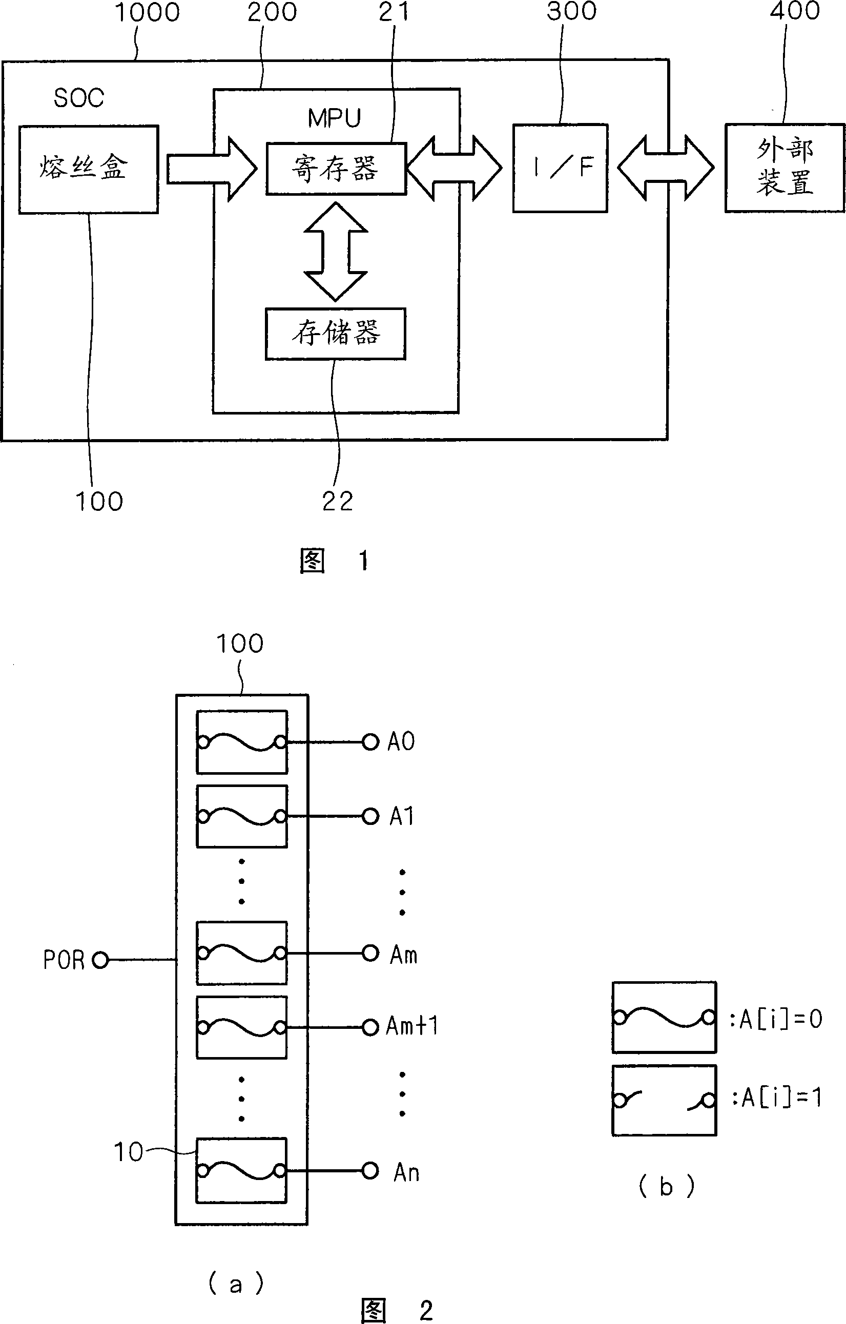
[0047] FIG. 1 is a block diagram showing the configuration of an SOC (system on chip) 1000 according to Embodiment 1. As shown in FIG.

[0048] As shown in FIG. 1 , SOC 1000 includes fuse box 100 , MPU (micro processing unit) 200 (calculation processing unit), and I / F (interface) unit 30 . The fuse box 100 has a plurality of fuses (not shown in FIG. 1 ) recording unique IDs, and each fuse corresponds to each bit of the unique ID. MPU 200 has registers 21 and memory 22 .

[0049] In FIG. 1 , the unique ID recorded in the fuse box 100 is read out to the register 21 of the MPU 200 and transferred to the external device 200 via the I / F 300 . Alternatively, the unique ID read to the register 21 may be stored in the memory 22 from the register 21 and processed, then read to the register 21 again, and then transferred to the external device 200 via the I / F 300 .

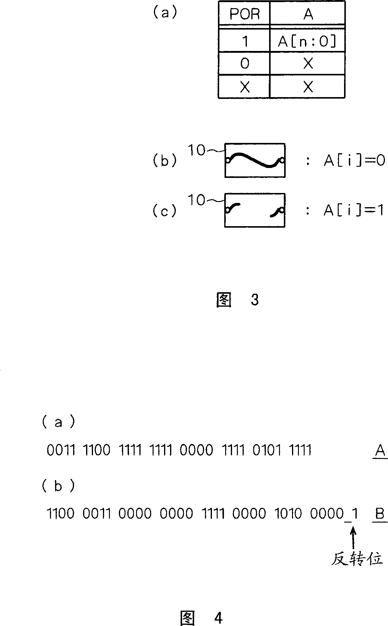
[0050] Fig. 2 (a) is the schematic diagram that shows the fuse box 100 that unique ID is installed on the SOC, is equip...

Embodiment approach 2

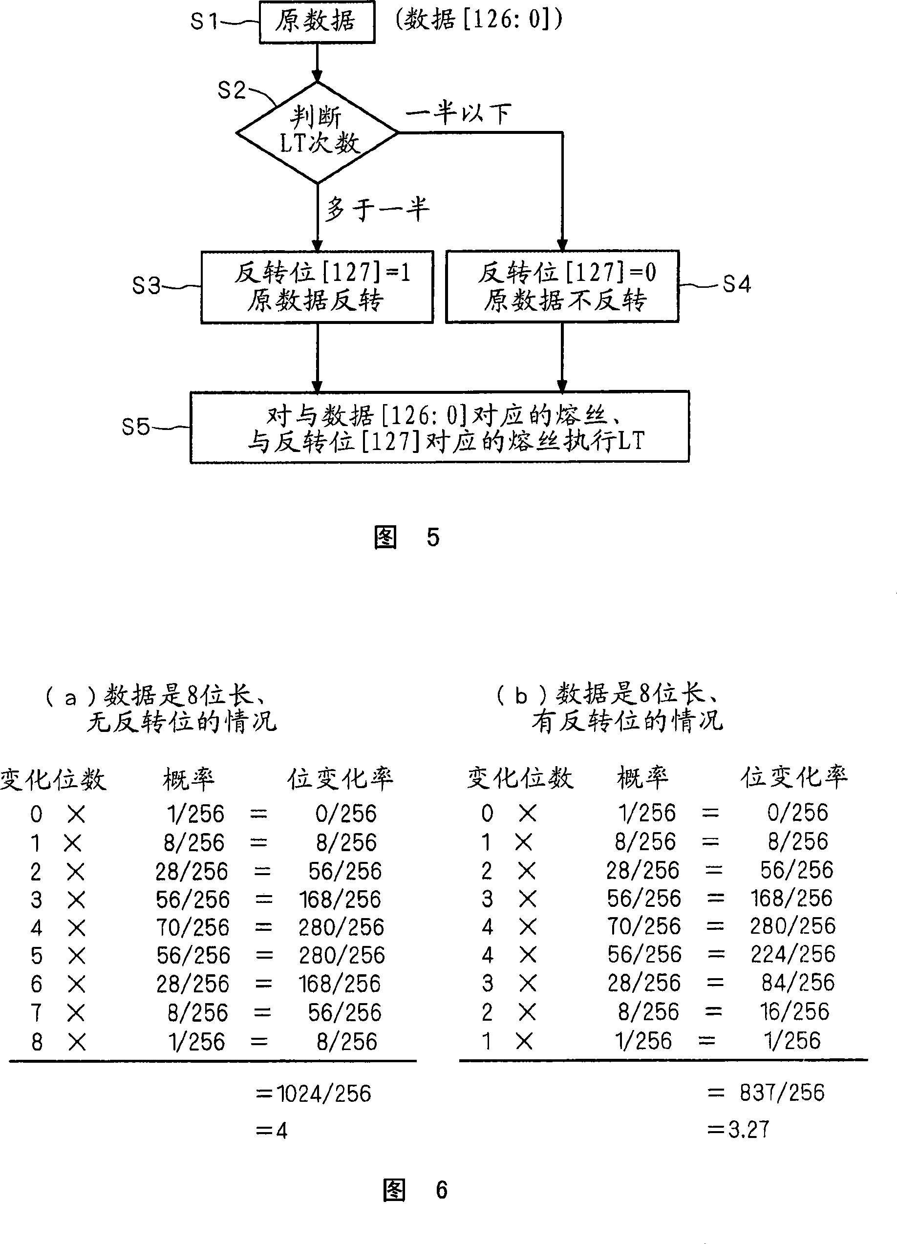
[0083] In Embodiment 1, the case where one inverted bit is set for the entire data composed of one bit string was described. However, the actually processed data may contain a very small portion of "1" bits. In this case, by excluding this portion from the target of bit inversion, it is possible to further reduce the number of LTs. . That is, one inverted bit can be set only for a part of the data composed of one bit string.

[0084] 8 is a flowchart showing one step (unique ID recording step) in the manufacturing method of the semiconductor device according to the second embodiment. In FIG. 8 , bit [n] which is an inverted bit is set to bit string [n-1:0] which is n-bit long data. The bit string [n-1:0] can be divided into m-bit long bit string [m-1:0] and (n-m) bit long bit string [n-1:m] (m is (n-1) or less natural number), the bit [n] which is the inverted bit is set only for the bit string [n-1:m]. That is, the flow chart of FIG. 8 adds step S1' to the flow chart of F...

Embodiment approach 3

[0091] In Embodiment 2, a case was described in which one inversion bit is set for data constituted by one bit string. However, the present invention is not limited thereto, and alternatively, two or more inverted bits may be set for data composed of one bit string.

[0092] 9 is a flowchart showing one step (unique ID recording step) in the manufacturing method of the semiconductor device according to the third embodiment. In FIG. 9 , bits [n-1], [n] which are inversion bits are set to bit string [n-2:0] which is data of (n-1) bit length. The bit string [n-2:0] can be divided into k-bit long bit string [k-1:0], (m-k) bit long bit string [m-1:k] and (n-m-1) bit long Bit string [n-2:m] (k is a natural number below (m-1)), set the bit [n-1] as the reverse bit only for the bit string [m-1:k], only for the bit String [n-2:m] sets bit [n] which is the inverted bit. That is, the flow chart of FIG. 9 takes steps S1-S4 in the flow chart of FIG. 1:k] and [n-2:m] individually.

[0...


PUM


Abstract

The present invention relates to a semiconductor device, a unique ID of the semiconductor device and a method for verifying the unique ID. Thus, original data (bit string) having 127-bit length [126:0] is inputted at step S1 . Then, it is determined whether the number of bits of ''1'' in the bit string [126:0] inputted at the step S 1 is more than the half of the bits of the bit string (that is, not less than 64) or not at step S2 . When the number is not less than 64, the process proceeds to step S3 . At the step S3 , the bit string [126:0] is inverted and an invert bit [127] is set to ''1''. Then, the process proceeds to step S5 . At the step S5 , the fuse corresponding to the bit string [126:0] and the bit [127] are cut by LT.

Description

technical field [0001] The present invention relates to a semiconductor device, a unique ID of a semiconductor device, and a method for verifying the unique (unique) ID, and in particular to a method for shortening the length of an SOC (system on chip) having a data recording unit of a fuse cutting type. The technology at the time of manufacture and the unique ID of the fuse installed. Background technique [0002] Conventionally, in order to implement a secure function in an SOC (system on chip), a method of attaching a unique identification number, that is, a unique ID uniquely assigned to each SOC has been employed (for example, Patent Document 1). [0003] Although this unique ID can be recorded in flash ROM (read only memory) or HDD (hard disk drive) constituting the system using the above-mentioned SOC, it must be mounted on a Recording in memory on the SOC is difficult. Therefore, in a general SOC manufacturing method, the following method is adopted: in the wafer t...

Claims


Application Information

Patent Timeline
Patent Type & Authority Applications(China)
IPC IPC(8): G06F21/00H01L23/544
CPCH01L2924/0002
Inventor 森保文东克彦三浦学
Owner RENESAS TECH CORP
Why Eureka
Try Eureka