

GESBTE thin film manufacturing method, phase-change direct-access storage and manufacturing method therefor
A manufacturing method and a random phase transition technology, which are applied in static memory, digital memory information, information storage, etc., can solve problems such as difficulty in forming GeSbTe thin films, and achieve the effect of good crystallinity and surface morphology
- Summary
- Abstract
- Description
- Claims
- Application Information
AI Technical Summary
Problems solved by technology
Method used
Image

Examples
Embodiment Construction
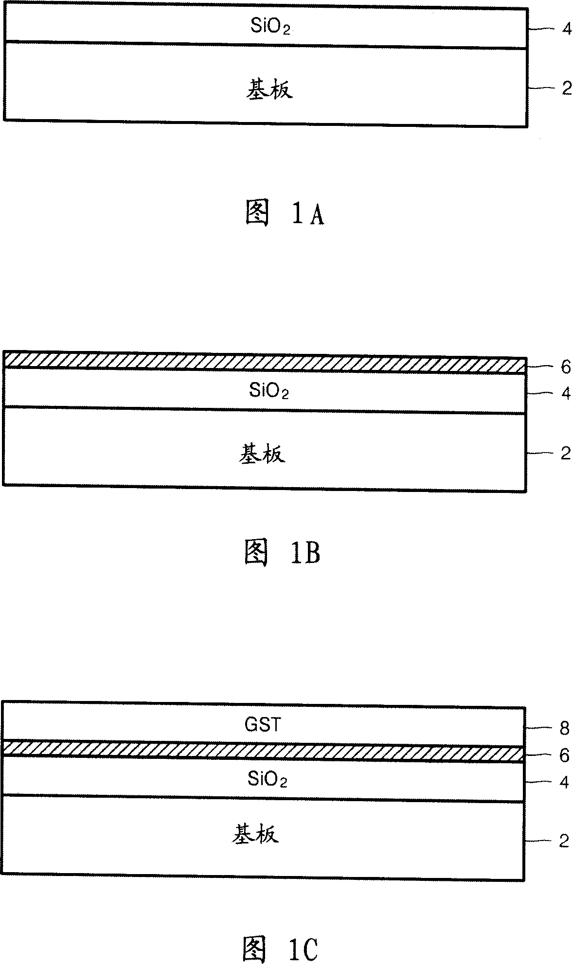
[0024] The invention will be described more fully hereinafter with reference to the accompanying drawings, in which preferred embodiments of the invention are shown. In the drawings, the thicknesses of layers and regions are exaggerated for clarity.
[0025] 1A, 1B and 1C are cross-sectional views illustrating a method of manufacturing a GeSbTe thin film according to an embodiment of the present invention. 1A to 1C, one or two selected from the group consisting of a Ge precursor, a Sb precursor and a Te precursor are supplied to the surface of an amorphous material layer 4 formed on a substrate 2, thereby forming a layer composed of Ge, Sb, Te, Sb 2 Te 3 Or the seed layer 6 made of Ge doped with Sb. Next, a Ge precursor, a Te precursor, and an Sb precursor are supplied to the surface of the seed layer 6 , thereby forming the GeSbTe thin film 8 . Here, the seed layer 6 has good adhesion to the amorphous material layer 4 and can provide nucleation sites for forming the GeSbT...
PUM
| Property | Measurement | Unit |
|---|---|---|
| thickness | aaaaa | aaaaa |
Abstract
Description
Claims
Application Information