
Patsnap Eureka
For R&D, Patsnap Eureka makes reading and utilizing patents & technical documents easy.
Patsnap Eureka AIR
Designed for self-driven R&D workflows. Generate viable solutions, solve complex R&D challenges, empower your innovation with AI.

Patsnap Eureka Materials
Designed for material experts only. Revolutionize your material R&D, from search, analyze, to developing new materials.

TechResearch
Generate reliable direction feasibility study reports for your R&D in just a few steps.

TechSeek
Discover and master advanced knowledge NOW. Basics, ideas, possibilities, all at once.

TechMind
As an expert in R&D Theories, TechMind can generates customized viable solutions instantly.

TechRisk
Analyze your overall solution with one click, know your potential R&D risks in advance.

TechMonitor
Get weekly tech updates, stay abreast of the latest tech innovations and key insights.
Thin-film transistor, pixel structure and LCD panel
A thin-film transistor and pixel structure technology, which is applied in the field of liquid crystal display panels, can solve problems such as cost increase, and achieve the effect of reducing cost and manufacturing cost
- Summary
- Abstract
- Description
- Claims
- Application Information
AI Technical Summary
Problems solved by technology
Method used
Image

Examples
Embodiment Construction
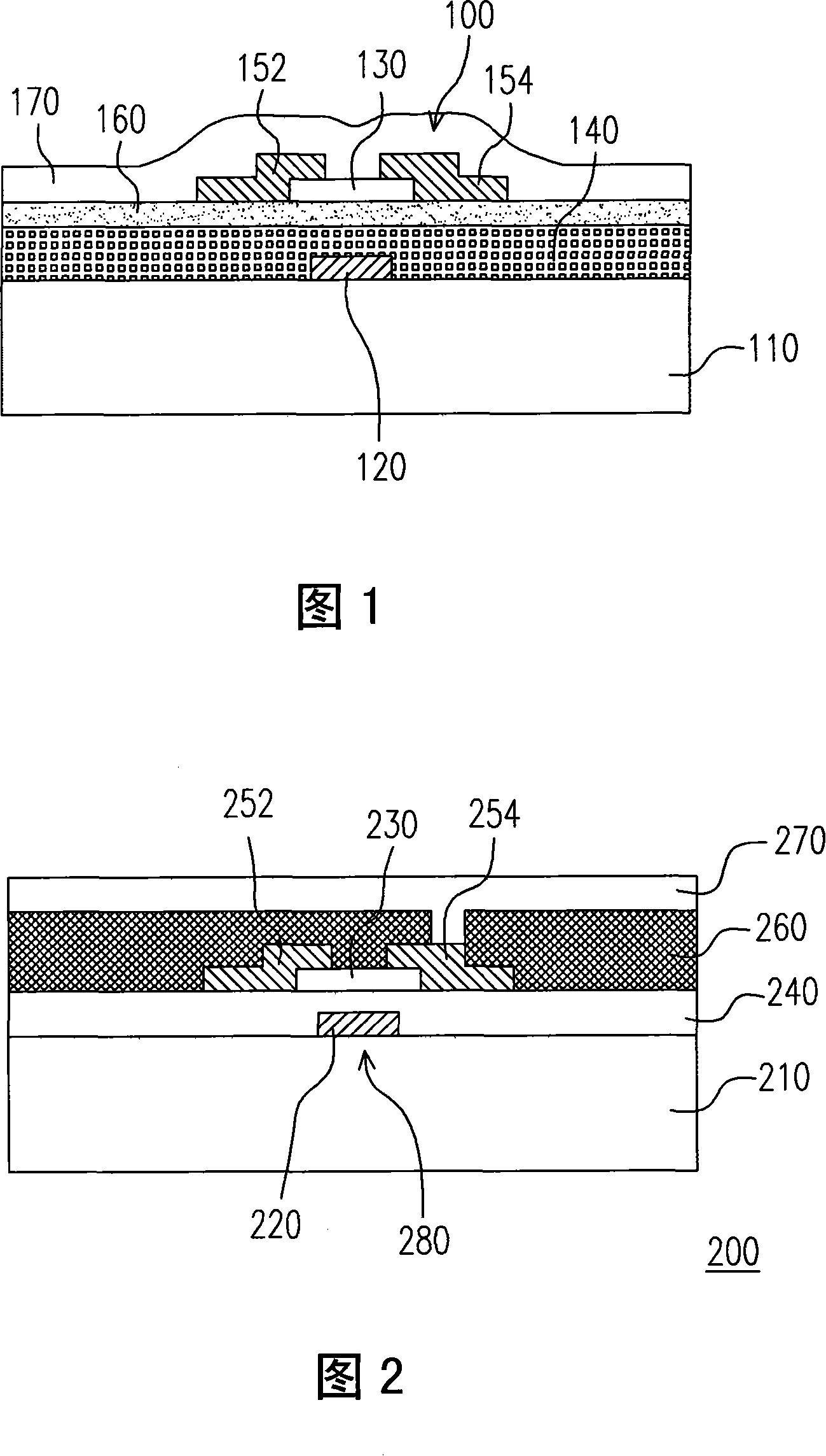
[0068] In the known thin film transistors, one or more insulating layers must be arranged to electrically insulate the gate from the source, drain and channel layers. Since there are various insulating materials that can convert light and filter light, the present invention proposes to use insulating materials that can make light appear in different colors to fabricate the insulating film layer of the thin film transistor and the pixel structure. In this way, the light can present a specific color after passing through the thin film transistor, pixel structure and related elements or display device of the present invention.
[0069] FIG. 1 shows a thin film transistor of an embodiment of the present invention. Referring to FIG. 1 , the thin film transistor 100 is disposed on a substrate 110 . The thin film transistor 100 includes a gate 120 , a semiconductor layer 130 , a gate insulating layer 140 , and a source 152 and a drain 154 . The gate insulation layer 140 is located ...
PUM
| Property | Measurement | Unit |
|---|---|---|
| diameter | aaaaa | aaaaa |
| diameter | aaaaa | aaaaa |
Abstract
Description
Claims
Application Information
 - R&D Engineer
- R&D Manager
- IP Professional
- Industry Leading Data Capabilities
- Powerful AI technology
- Patent DNA Extraction
Browse by: Latest US Patents, China's latest patents, Technical Efficacy Thesaurus, Application Domain, Technology Topic, Popular Technical Reports.
© 2024 PatSnap. All rights reserved.Legal|Privacy policy|Modern Slavery Act Transparency Statement|Sitemap|About US| Contact US: help@patsnap.com