Liquid crystal display element, electronic device, and manufacturing method of liquid crystal display element
A technology of liquid crystal display elements and liquid crystal molecules, applied in nonlinear optics, instruments, optics, etc., can solve the problems of retardation layer damage, damage to display characteristics, etc., and achieve the effect of improved orientation, good viewing angle, and high contrast display
- Summary
- Abstract
- Description
- Claims
- Application Information
AI Technical Summary
Problems solved by technology
Method used
Image

Examples
no. 1 approach
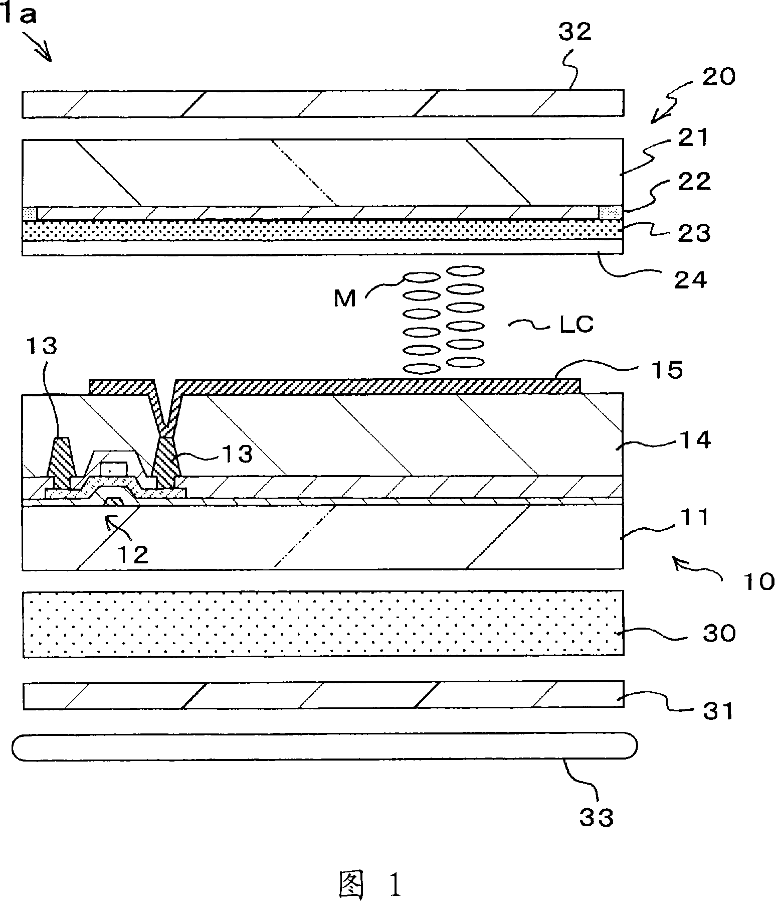
[0038] FIG. 1 is a cross-sectional configuration diagram of a liquid crystal display element 1a of the first embodiment. The liquid crystal display element 1a shown in the figure has a retardation layer (hereinafter referred to as a hybrid retardation layer) for hybrid alignment of liquid crystal molecules, and this liquid crystal display element is a transmissive liquid crystal display element 1a driven in the ECB mode, and is configured as follows .
[0039] That is, the liquid crystal display element 1 a includes a drive substrate 10 , a counter substrate 20 disposed opposite to the element forming surface of the drive substrate 10 , and a liquid crystal layer LC sandwiched between the drive substrate 10 and the counter substrate 20 . In addition, a λ / 4 retardation layer 30 is provided on the outer surface of the drive substrate 10 in a closely bonded state, and the outer surfaces of the drive substrate 10 and the counter substrate 20 are crossed in a closely bonded state. ...
no. 2 approach
[0072] FIG. 5 is a cross-sectional configuration diagram of a liquid crystal display element 1b of the second embodiment. The difference between the liquid crystal display device 1b shown in this figure and the liquid crystal display element of the first embodiment described with reference to FIG. the same way.
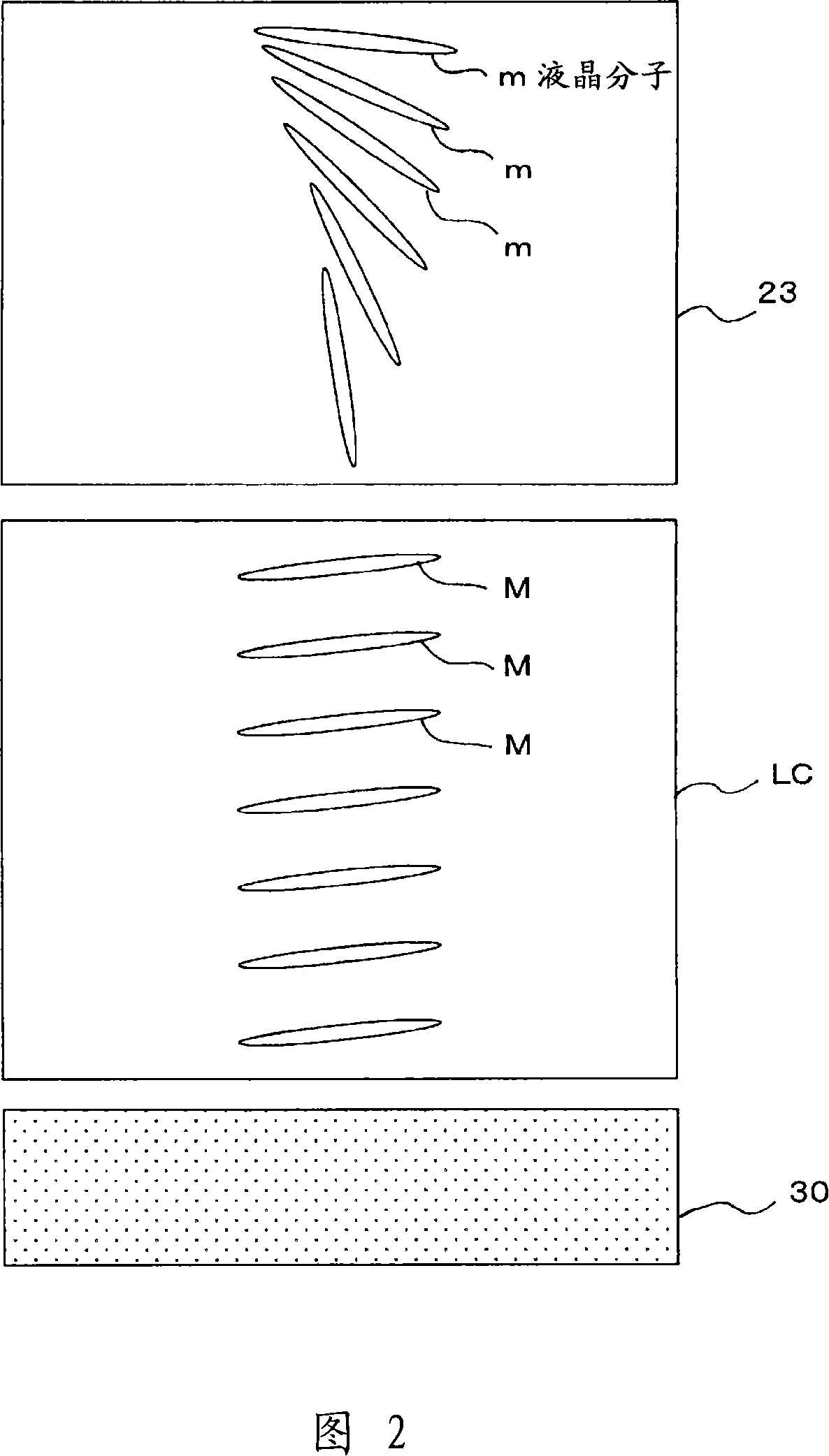
[0073] That is, the second embodiment is characterized in that the hybrid retardation layer 23 is a layer formed by forming a film on the surface of the transparent substrate 21 facing the liquid crystal layer LC side on the counter substrate 20 side. Therefore, as shown in FIG. 6 , the liquid crystal particles m of the hybrid retardation layer 23 are horizontal on the transparent substrate side of the counter substrate, and gradually become vertically erect toward the liquid crystal layer LC side. Further, in this liquid crystal display element 1b, layers having a retardation are provided in order from the backlight side in the order of the liquid crystal layer LC, ...
no. 3 approach
[0080] FIG. 7 is a cross-sectional configuration diagram of a liquid crystal display element 1c of the third embodiment. The liquid crystal display element 1c shown in the drawing is different from the liquid crystal display element explained using FIG. , the other structures are the same as those of the first embodiment.
[0081] That is, in this third embodiment, it is characterized in that the hybrid retardation layer 23 and the λ / 4 retardation layer 30' are formed by film formation on the surface of the transparent substrate 21 facing the liquid crystal layer LC side on the counter substrate 20 side. layer. In addition, referring to FIG. 6 above, the liquid crystal particles m of the hybrid retardation layer 23 are horizontal on the transparent substrate side of the counter substrate, and gradually become a vertical vertical alignment state toward the liquid crystal layer LC side.
[0082] On the other hand, the ? / 4 retardation layer 30' may be a general uniformly orient...
PUM
 Abstract
Description
Claims
Application Information
 - R&D
- Intellectual Property
- Life Sciences
- Materials
- Tech Scout
- Unparalleled Data Quality
- Higher Quality Content
- 60% Fewer Hallucinations
Browse by: Latest US Patents, China's latest patents, Technical Efficacy Thesaurus, Application Domain, Technology Topic, Popular Technical Reports.
© 2025 PatSnap. All rights reserved.Legal|Privacy policy|Modern Slavery Act Transparency Statement|Sitemap|About US| Contact US: help@patsnap.com