Semiconductor device and its making method

A semiconductor and oxide semiconductor technology, applied in semiconductor/solid-state device manufacturing, semiconductor devices, electrical components, etc., to achieve the effects of avoiding silicon loss and thermal budget, low contact resistance, and low thermal budget

Active Publication Date: 2008-02-13
SEMICON MFG INT (SHANGHAI) CORP +1
View PDF1 Cites 21 Cited by
  • Summary
  • Abstract
  • Description
  • Claims
  • Application Information

AI Technical Summary

Problems solved by technology

Therefore, integrating NiSi into the overall process flow remains

Method used


Image

  • Semiconductor device and its making method
  • Semiconductor device and its making method
  • Semiconductor device and its making method

Examples


Embodiment Construction

[0056] In order to make the above objects, features and advantages of the present invention more comprehensible, specific implementations of the present invention will be described in detail below in conjunction with the accompanying drawings.

[0057] In the following description, numerous specific details are set forth in order to provide a thorough understanding of the present invention. However, the present invention can be implemented in many ways other than those described here, and those skilled in the art can make similar extensions without departing from the connotation of the present invention. Accordingly, the invention is not limited to the specific implementations disclosed below.

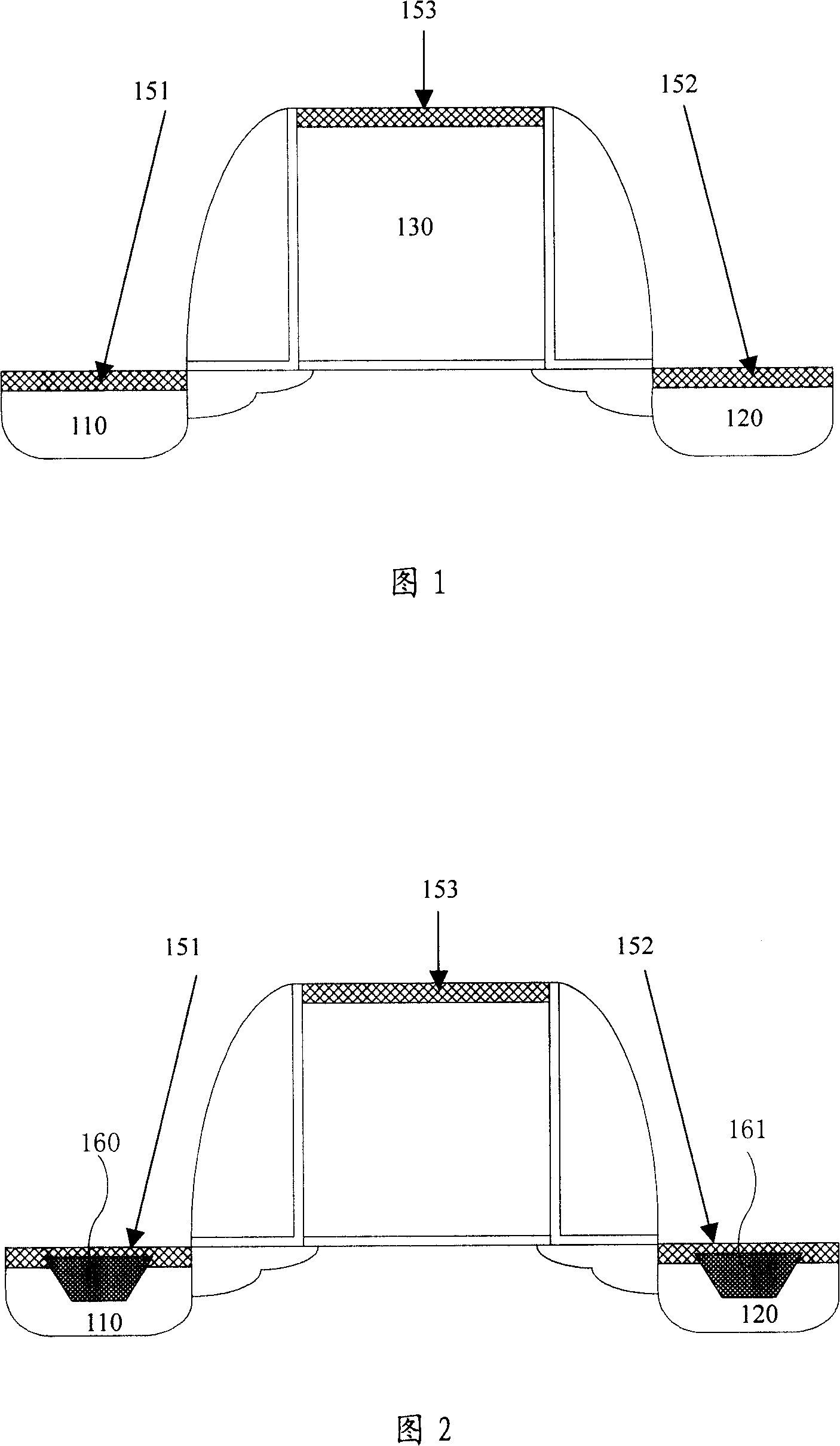
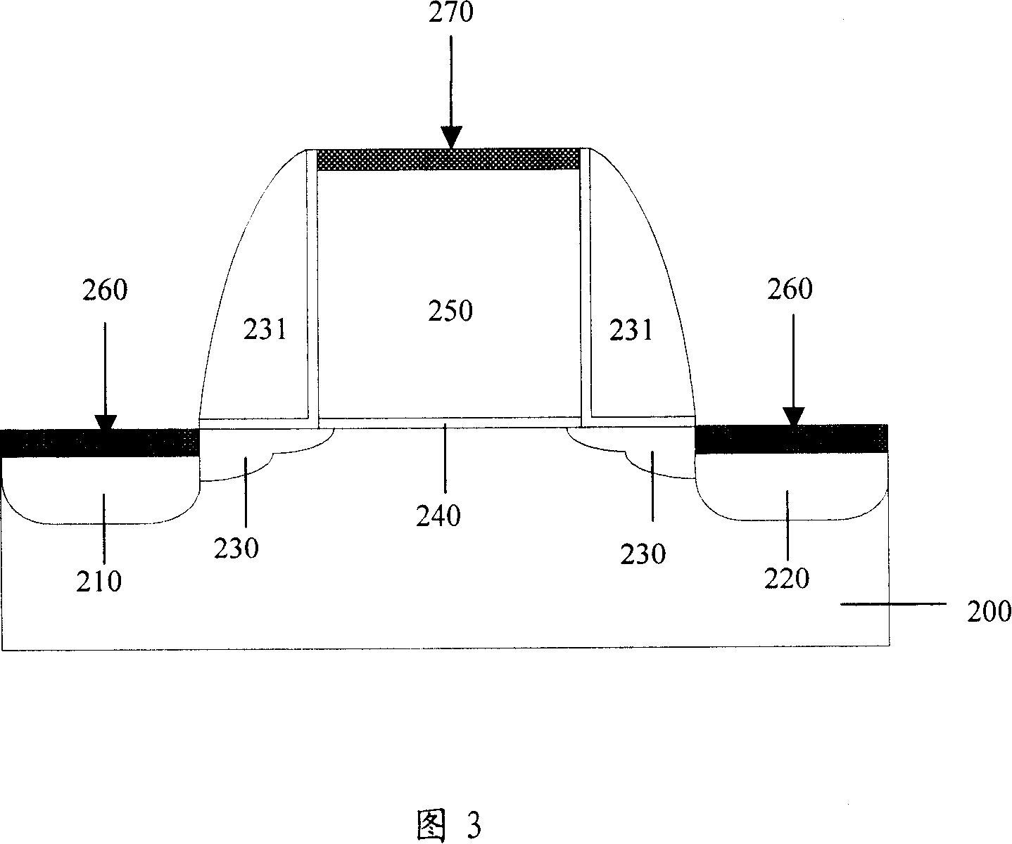
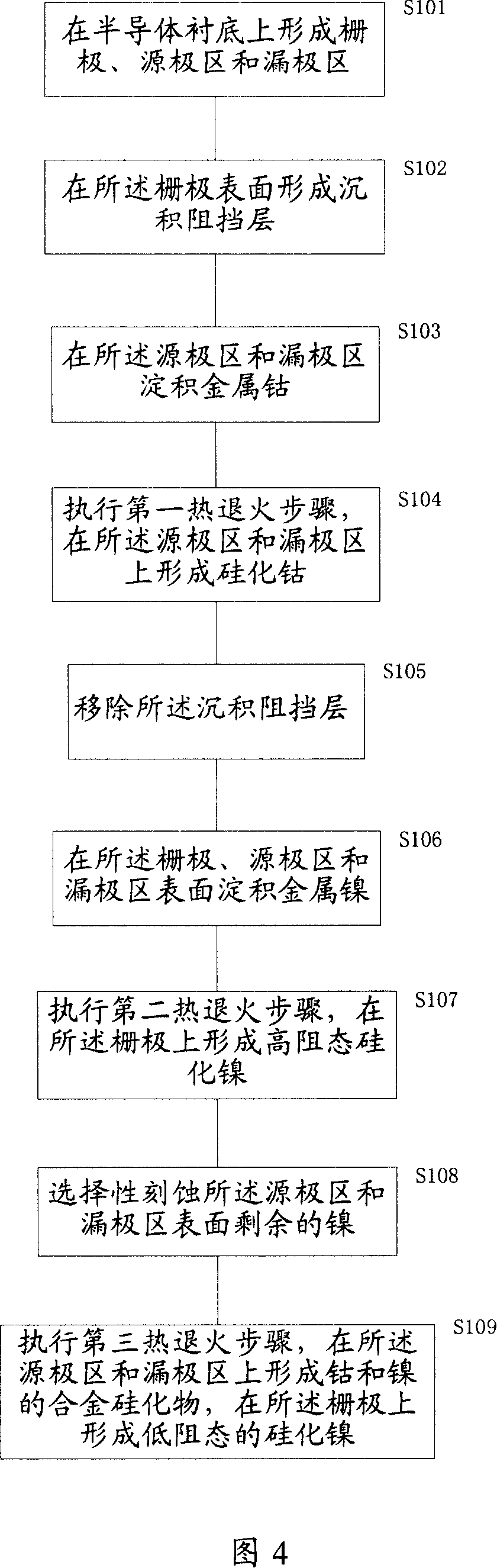
[0058] The semiconductor device and its manufacturing method provided by the invention are especially suitable for semiconductor devices with a feature size of 65nm or below and its manufacturing. The semiconductor device is not only a MOS transistor, but also a PMOS transistor and an...


PUM


Abstract

The invention discloses a metal oxide semi-conductor device, which comprises a semi-conductor underlayer, a grid structure formed on the surface of the underlayer, and the two sides of which have side wall isolators, a source electrode area and a drain electrode area positioned on the two sides of the side wall isolators on the underlayer, a first metal silicide positioned on the source electrode area and the drain electrode area, and a second silicide positioned on the grid structure. The manufacturing method of semi-conductor devices of the invention forms respectively the first metal silicide containing the first and the second metal, and forms the second silicide containing the second metal. The invention combines the advantages of both the cobalt silicide techniques and the nickel silicide techniques, and applies well the nickel silicide techniques to the following technique nodes below 65nm. The invention reduces the risk of forming spriking in the source/drain area, when assuring the formation of metal contact layer of high reliability on the surface of the grid by using nickel silicide.

Description

technical field [0001] The invention relates to the technical field of semiconductor manufacturing, in particular to a metal contact layer of a metal oxide semiconductor field effect transistor (MOS) and a manufacturing method thereof. Background technique [0002] In ultra-high-speed MOS large-scale integrated circuits, in order to reduce the sheet resistance and parasitic resistance of source / drain electrodes and gates, a self-aligned silicide (salicide) process is used. In the self-alignment technology, a reaction product of a metal and a semiconductor such as silicon (Si) is formed on the source and drain regions of a MOSFET composed of an impurity diffusion layer formed on a semiconductor substrate and a gate electrode composed of polysilicon. Silicide (hereinafter referred to as metal silicide). Metal suicide plays a very important role in VLS / ULSI device technology. In MOS devices, metal silicides are often used to obtain good low resistance contacts. Metal silicid...

Claims


Application Information

Patent Timeline
IPC IPC(8): H01L29/78H01L29/43H01L29/49H01L21/336H01L21/28
CPCH01L29/665H01L29/7833H01L29/4933
Inventor 吴汉明宁先捷
Owner SEMICON MFG INT (SHANGHAI) CORP
Why Eureka
Try Eureka