Temperature control device of etching equipment and its method for controlling wafer temperature

A technology of etching equipment and temperature control device, which is applied in the field of temperature control system, can solve the problems that the edge of the wafer cannot be cooled, the gas volume cannot be controlled and measured, and the pressure of the back cooling gas is affected, so as to change the heat dissipation effect and structure. Simple, temperature-controlled effects

Active Publication Date: 2008-02-27
BEIJING NAURA MICROELECTRONICS EQUIP CO LTD
View PDF0 Cites 19 Cited by
  • Summary
  • Abstract
  • Description
  • Claims
  • Application Information

AI Technical Summary

Problems solved by technology

[0011] One is to let the backcooled gas leak at the edge of the electrostatic chuck to improve the heat dissipation performance of the edge of the wafer, but in this method, the gas leaked from the edge is connected to the gas in the center of the wafer and other parts, so The amount of leaked gas cannot be controlled and measured, and if the amount of leaked gas is too large, it will inevitably affect the pressure of backcooled gas in other parts, making it difficult to control the temperature of the wafer
[0012] The other is to design back-cooled gas leakage holes on the side of the electrostatic chuck, but the function of the back-cooled gas leakage holes is mainly to stabilize the pressure of the back-cooled gas, so those back-cooled gas holes communicate with the surface of the electrostatic chuck Yes, the amount of leakage is very small, just to stabilize the pressure of the back-cooled back-cooled gas, and it cannot cool the edge of the wafer

Method used


Image

  • Temperature control device of etching equipment and its method for controlling wafer temperature
  • Temperature control device of etching equipment and its method for controlling wafer temperature

Examples


specific Embodiment approach 1

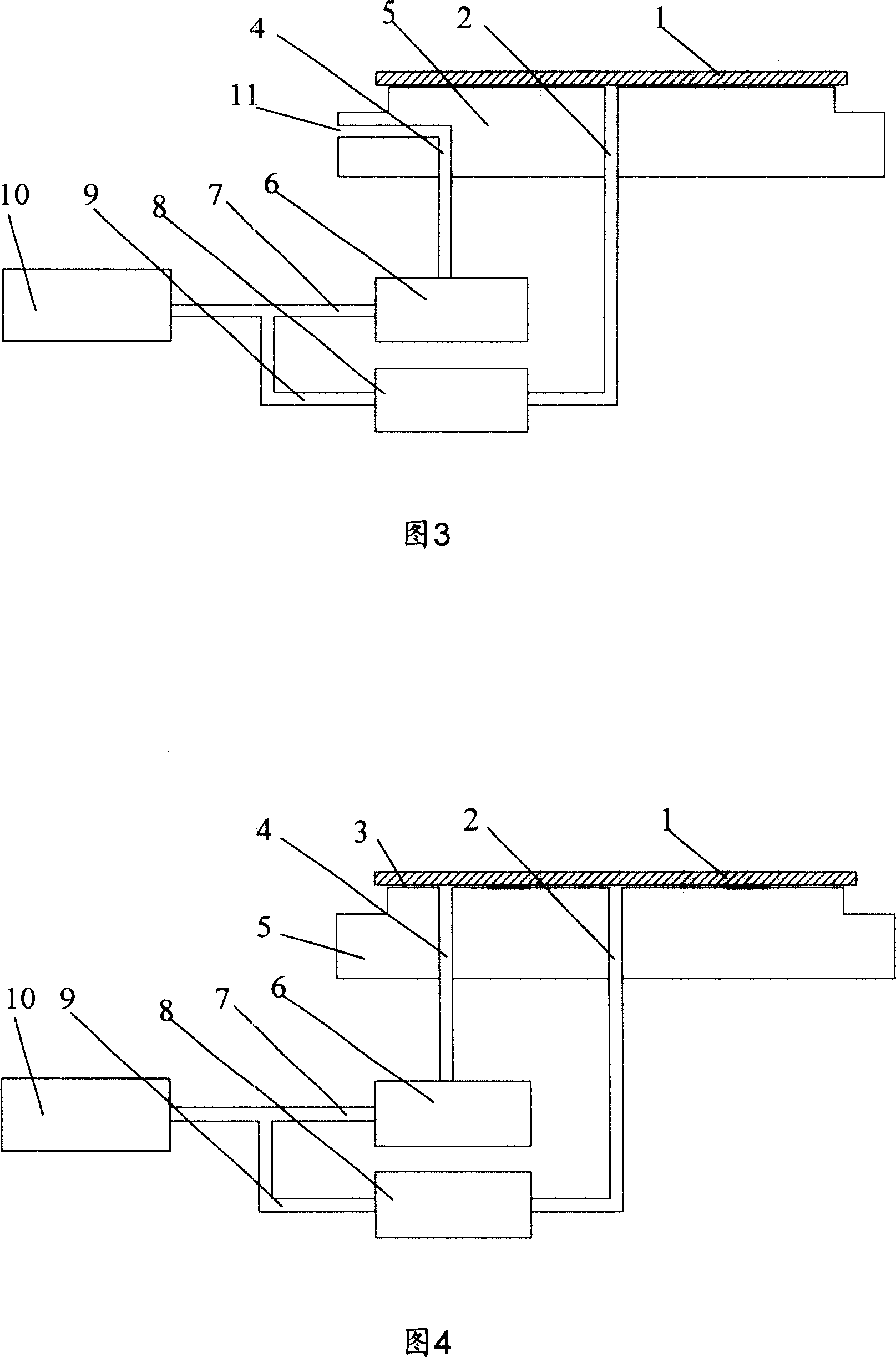
[0041] For this reason, preferred specific implementation mode 1 that the present invention adopts, as shown in Figure 3:

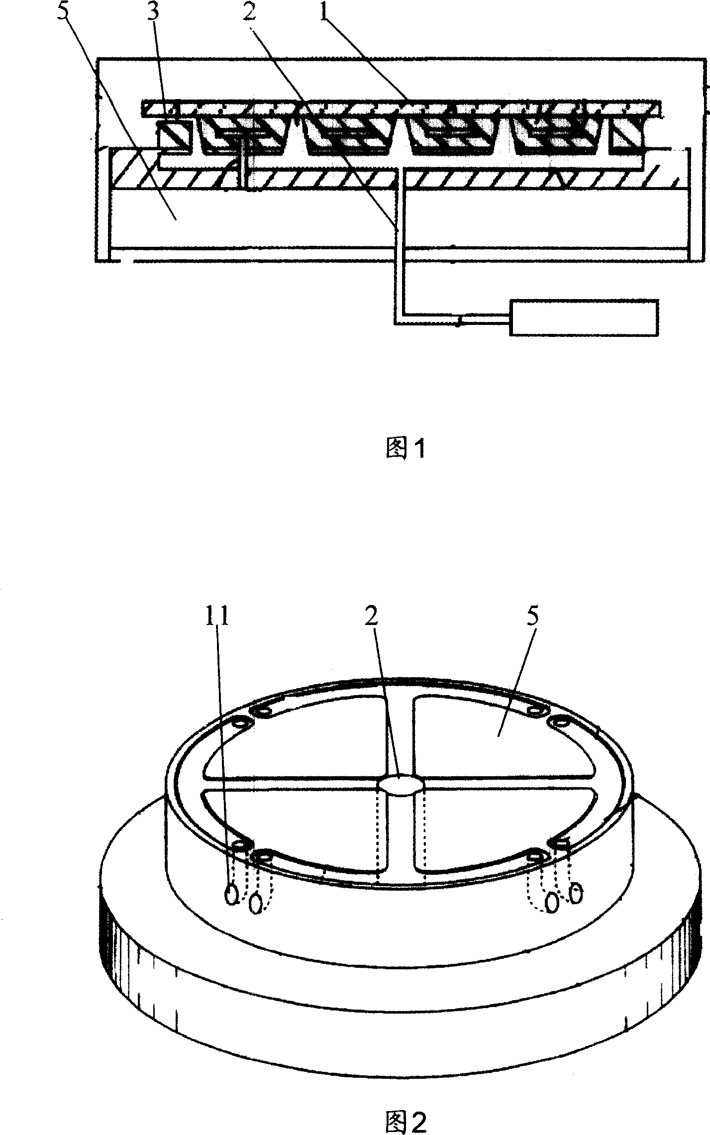
[0042] One or more back cooling gas leakage holes 11 are provided on the edge of the electrostatic chuck 5 , the back cooling gas leakage holes 11 communicate with the edge back cooling gas channel 4 , and the back cooling gas can leak along the edge back cooling gas channel 4 partly.

[0043] The first preferred specific implementation mode adopted by the present invention, as shown in Figure 4:

[0044] At the edge of the electrostatic chuck 5 , specifically at the edge of the edge back cooling gas channel 4 , the part of the contact surface 3 that is in contact with the wafer 1 is slightly rough, and the back cooling gas can leak along the rough surface 3 .

[0045]The central back-cooled gas channel 2 is connected to the central gas path 9 , and the edge back-cooled gas channel 4 is connected to the edge gas path 7 . A pressure controller 8 is provid...


PUM


Abstract

The present invention discloses a temperature-controlling device of an etching device and method of controlling the wafer temperature, and includes electrostatic chuck on which the wafer can be placed. The unconnected central and side back-cool-gas channels are set on the electrostatic chuck; the central back-cool-gas channel partly intimately contacts with the wafer, and is well sealed; margin of the side back-cool-gas channel, which partly contacts the wafer, is a little rough, or a or several back-cool-gas leak holes are set on the margin of electrostatic chuck; the back-cool gas in the side back-cool-gas channel can leak along the rough surface or the leak holes; the central back-cool-gas channel connects a pressure controller; the side back-cool-gas channel connects a mass and flux controller. The present invention has simple structure and is easy to use; heat-dissipated effect of wafer margin can be changed, and temperature of wafer can also be controlled. The present invention is mainly applied to the temperature-controlling system in semiconductor processing.

Description

technical field [0001] The invention relates to a temperature control system in a semiconductor production process, in particular to a temperature control device of wafer etching equipment and a method for controlling the temperature of the wafer. Background technique [0002] Chucks are used in semiconductor manufacturing processes to hold and support wafers to prevent wafer movement or misalignment during processing. Electrostatic chucks use electrostatic attraction to hold wafers and offer many advantages over previously used mechanical and vacuum chucks. The electrostatic chuck reduces wafer damage caused by pressure, collision, etc. when using a mechanical chuck; increases the area where the wafer can be effectively processed; reduces the deposition of corrosion particles on the wafer surface; and can be used in a vacuum process environment Work. [0003] A typical electrostatic chuck consists of a base and an electrostatic module fixed on it. The electrostatic modul...

Claims


Application Information

Patent Timeline
Patent Type & Authority Applications(China)
IPC IPC(8): H01L21/00H01L21/3065H01L21/683C23F4/00
CPCH01L21/67248H01L21/6831H01L21/00H01L21/683H01L22/00
Inventor 刘利坚
Owner BEIJING NAURA MICROELECTRONICS EQUIP CO LTD
Why Eureka
Try Eureka