Non-pin packaging structure of semiconductor element and packaging technology thereof
A packaging structure and semiconductor technology, applied in semiconductor devices, semiconductor/solid-state device manufacturing, semiconductor/solid-state device components, etc. Eliminate problems such as falling off, achieve the effects of saving development costs, improving reliability, and enhancing binding force
- Summary
- Abstract
- Description
- Claims
- Application Information
AI Technical Summary
Problems solved by technology
Method used
Image

Examples
Embodiment 1
[0050] Process example 1: Engraving first and then plating
[0051] The encapsulation process of the semiconductor device of the present invention without feet encapsulation comprises the following steps:
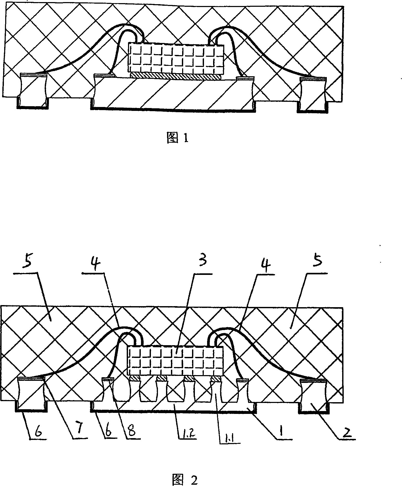
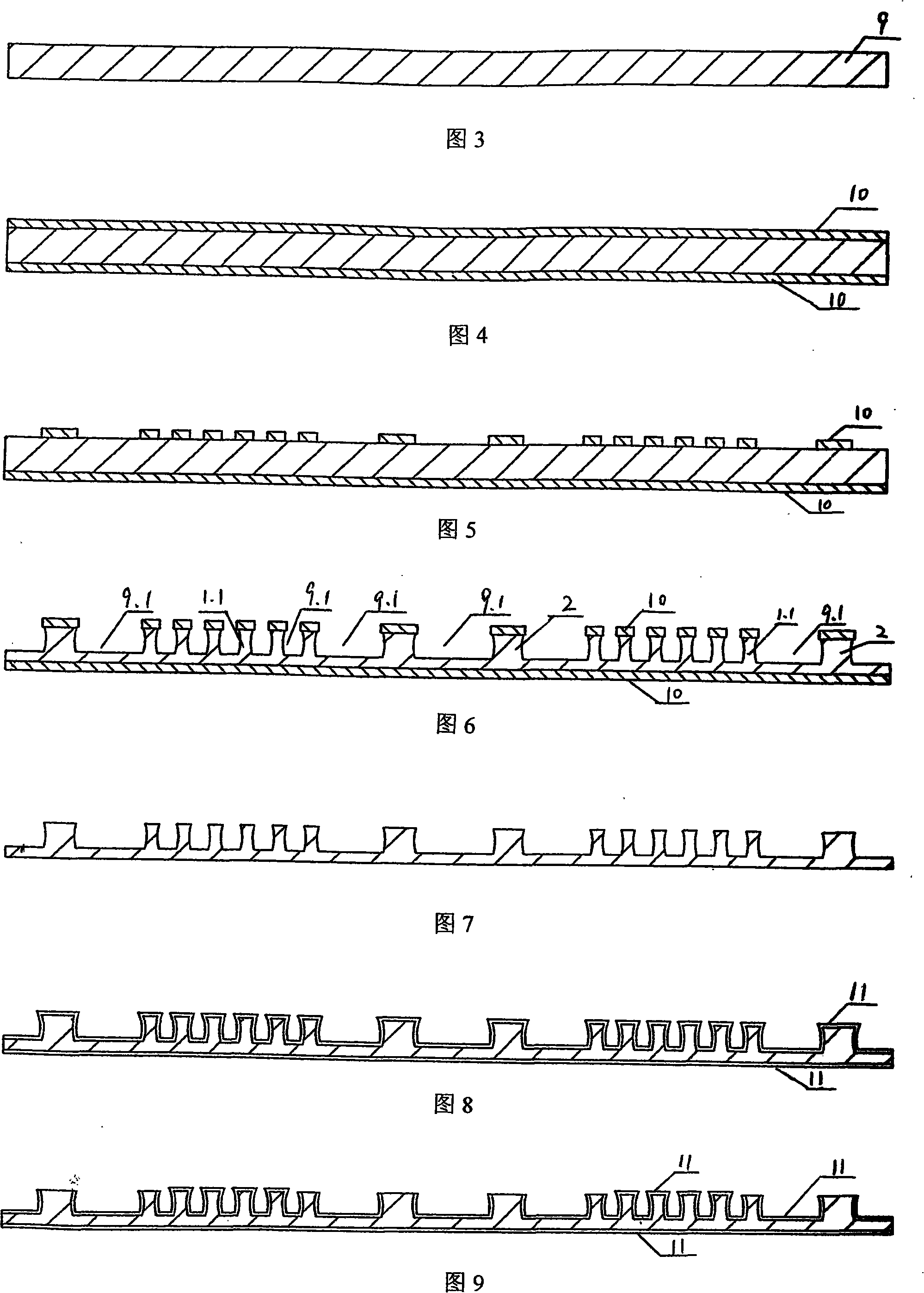
[0052] ——Take a piece of metal substrate 9, as shown in Figure 3;
[0053] ——Affix a mask 10 on the front and back sides of the metal substrate 9 to protect the subsequent etching process, as shown in Figure 4;
[0054] ——Removing part of the mask 10 on the front of the metal substrate 9, the intention is to expose the area on the metal substrate to be half-etched, as shown in Figure 5;
[0055] - Half-etching the area where the mask was removed in the previous process, forming a recessed half-etching area 9.1 on the front surface of the metal substrate 9, and at the same time forming a relatively preliminary bump-shaped wiring pin carrying base 2 and a plurality of chip carrying bases An independent metal bump 1.1, as shown in Figure 6;
[0056] ——Remove the remaining mas...
Embodiment 2
[0072] Process Example 2: Engraving after Plating
[0073] The engraving and engraving engraving process after the first plating of the semiconductor device of the present invention includes the following steps:
[0074] ——Take a piece of metal substrate 9, as shown in Figure 3;
[0075] ——Affix a mask 10 on the front and back sides of the metal substrate 9 to protect the subsequent etching process, as shown in Figure 4;
[0076] ——Remove part of the mask 10 on the front of the metal substrate 9 to expose the area on the metal substrate to be plated with a metal layer, as shown in Figure 5-1;
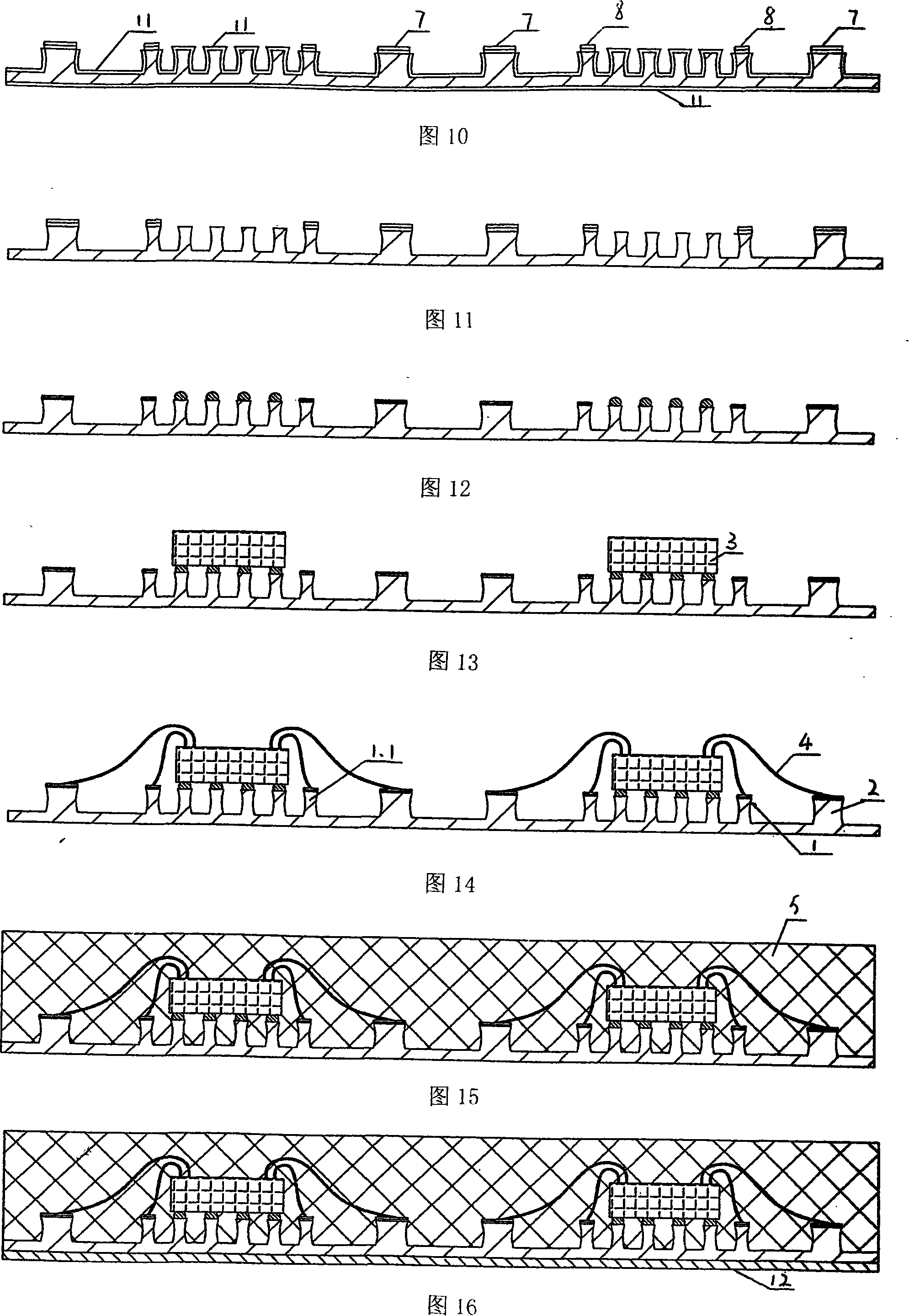
[0077] ——Carry out the metallization operation on the area where the mask was removed in the previous process, and form metal layer II7 and metal layer III8 on the front of the metal substrate 9, as shown in Figure 6-1;
[0078] ——Remove the remaining mask 10 on the front of the metal substrate and the mask 10 on the back of the metal substrate, as shown in Figure 7-1;
[0079] - Cov...
PUM
 Abstract
Description
Claims
Application Information
 - Generate Ideas
- Intellectual Property
- Life Sciences
- Materials
- Tech Scout
- Unparalleled Data Quality
- Higher Quality Content
- 60% Fewer Hallucinations
Browse by: Latest US Patents, China's latest patents, Technical Efficacy Thesaurus, Application Domain, Technology Topic, Popular Technical Reports.
© 2025 PatSnap. All rights reserved.Legal|Privacy policy|Modern Slavery Act Transparency Statement|Sitemap|About US| Contact US: help@patsnap.com