Cleaning apparatus and cleaning method

A washing device and washing method technology, which are applied in chemical instruments and methods, cleaning methods and utensils, and cleaning methods using liquids, etc., can solve problems such as lowering the yield of semiconductor devices, and achieve a simple structure and prevent the lowering of the yield. Effect

Inactive Publication Date: 2008-03-05
TOKYO ELECTRON LTD
View PDF11 Cites 10 Cited by
  • Summary
  • Abstract
  • Description
  • Claims
  • Application Information

AI Technical Summary

Problems solved by technology

When the particles are attached to the surface of the substrate, a circuit short occurs on a product (such as

Method used


Image

  • Cleaning apparatus and cleaning method
  • Cleaning apparatus and cleaning method
  • Cleaning apparatus and cleaning method

Examples


Embodiment Construction

[0063] Hereinafter, embodiments of the present invention will be described with reference to the drawings.

[0064] First, a substrate processing apparatus using a cleaning apparatus according to an embodiment of the present invention will be described.

[0065] FIG. 1 is a cross-sectional view showing a schematic configuration of a substrate processing apparatus using a cleaning apparatus according to an embodiment of the present invention.

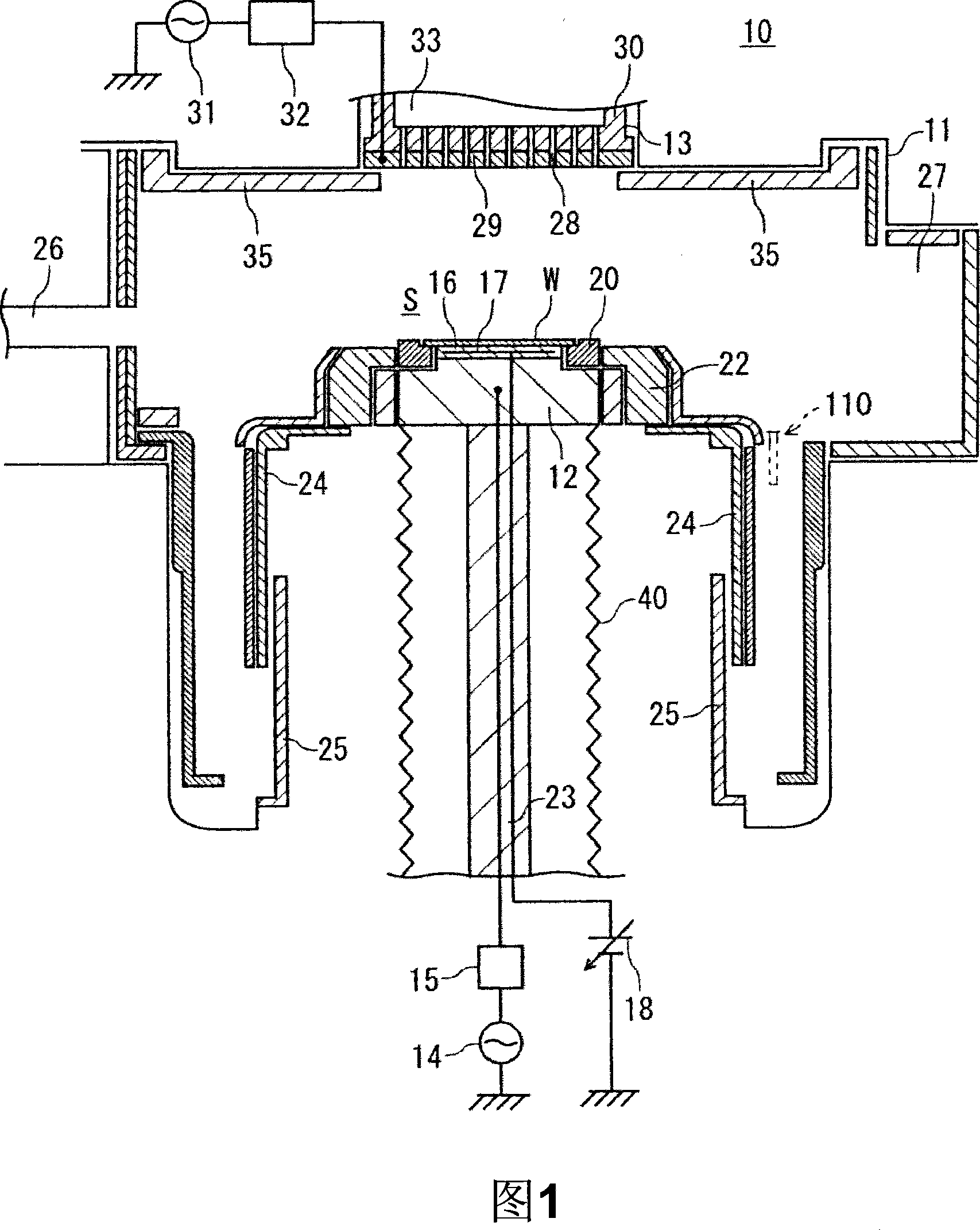
[0066] In FIG. 1 , substrate processing is configured as an etching processing apparatus for performing plasma processing on a semiconductor device wafer W (hereinafter simply referred to as "wafer W"), for example, reactive ion etching (Reactive Ion Etching) processing. The apparatus 10 has a chamber 11 as a processing chamber made of metal such as aluminum or stainless steel.

[0067] A lower electrode 12 and a shower head 13 are arranged in the chamber 11 . The lower electrode 12 serves as a stage on which a wafer W having a diamete...


PUM


Abstract

A cleaning apparatus which can efficiently and satisfactorily clean component parts facing towards narrow spaces. A cleaning apparatus (100) is arranged with main body (120) and two-layer tube nozzle (110) extending freely from the main body (120). The two-layer tube nozzle (110) is arranged with ejecting tube (114) and suction catheter (112) surrounding the ejecting tube (112), the ejecting mouth (114a) of the ejecting tube (114) opens within the suction (112a) of the suction catheter (112). The ejecting tube (114) is arranged with reduced section (114b) by its ejecting mouth (114a), and accelerates the gas within the reduced section (114b). As a result, to gel part of gas, and the gas forms bow wave due to acceleration. Thus, the ejecting tube (114) ejects the bow wave containing the gas and air sol composed of material being same to the gas, towards particle (P) hanging to the surface of a construction (50).

Description

technical field [0001] The present invention relates to a cleaning device and a cleaning method, in particular to a cleaning device and a cleaning method for cleaning a small space in a semiconductor device manufacturing device. Background technique [0002] Generally, a substrate processing apparatus for performing predetermined processing on a substrate such as a wafer for a semiconductor device has a processing chamber (hereinafter referred to as a "chamber") for accommodating a substrate and performing predetermined processing. Adhesions caused by reaction products generated in predetermined processes adhere to the chamber. These attached deposits are suspended as particles. When the particles adhere to the surface of the substrate, a line short occurs on a product (such as a semiconductor device) manufactured from the substrate, and the yield of the semiconductor device decreases. Then, in order to remove the deposits in the chamber, maintenance such as wet cleaning i...

Claims


Application Information

Patent Timeline
IPC IPC(8): B08B7/00B08B7/04
CPCB08B3/02H01L21/02041H01L21/67051
Inventor 守屋刚
Owner TOKYO ELECTRON LTD
Why Eureka
Try Eureka