Heat radiation substrate of electronic element

A technology of electronic components and substrates, which is applied in the field of heat dissipation substrates for heat dissipation of electronic components, and can solve problems such as insufficient heat dissipation requirements

Inactive Publication Date: 2008-03-12
POLYTRONICS TECH
View PDF0 Cites 31 Cited by
  • Summary
  • Abstract
  • Description
  • Claims
  • Application Information

AI Technical Summary

Problems solved by technology

However, with the widespread application of high-power LEDs, their operating current can reach more than 1A, and the conventional printed circuit boa...

Method used


Image

  • Heat radiation substrate of electronic element

Examples


Embodiment Construction

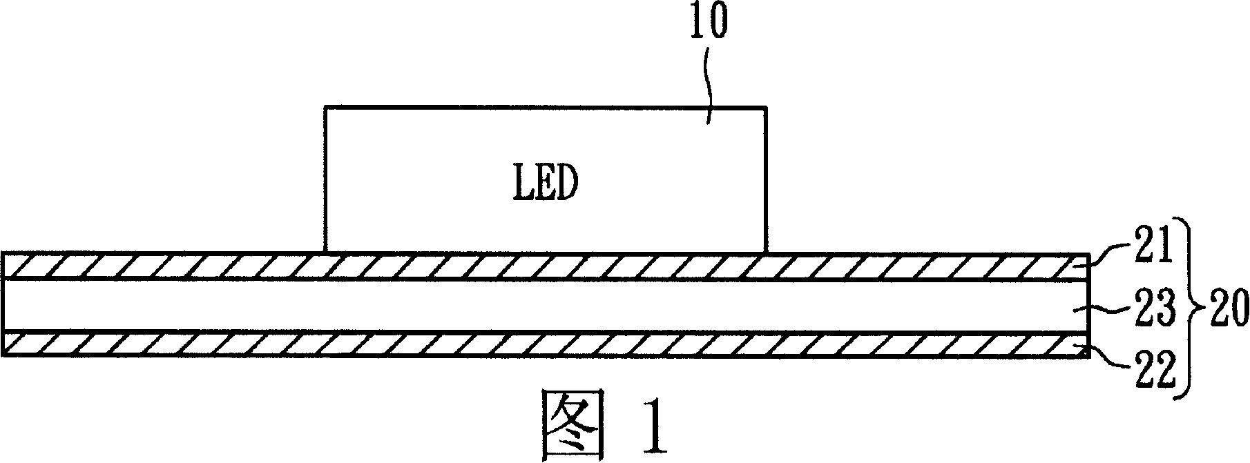
[0012] Referring to FIG. 1 , an LED element 10 is carried on a heat dissipation substrate 20 . The heat dissipation substrate 20 includes a first metal layer 21 , a second metal layer 22 and a thermally conductive polymer dielectric insulating material layer 23 stacked between the first metal layer 21 and the second metal layer 22 . The LED element 10 is disposed on the surface of the first metal layer 21, and the interface between the first and second metal layers 21 and 22 forms a physical contact with the thermally conductive polymer dielectric insulating material layer 23, and wherein At least one interface is a micro-rough surface, and the micro-rough surface includes a plurality of tumor-like protrusions, and the particle diameters of the nodule-like protrusions are mainly distributed between 0.1 and 100 microns, thereby increasing the tensile strength between them.

[0013] The manufacturing method of the above-mentioned heat dissipation substrate 20 is exemplified as f...


PUM

PropertyMeasurementUnit
Particle sizeaaaaaaaaaa
Thermal conductivityaaaaaaaaaa
Thicknessaaaaaaaaaa

Abstract

A thermolytic underlay of the electronic component comprises a first metal layer, a second metal layer and a heat-conducting macromolecule dielectric insulated material layer. The said first metal layer surface bears the said electronic component like the LED component. The heat-conducting macromolecule dielectric insulated material layer is lapped between the first and second metal layer to form physical contact, wherein the interface includes at least one slightly rugged face with the roughness concentration larger than 7.0 Rz. The said slightly rugged face includes a plurality of grain diameters of the strumae mainly distributed between 0.1 and 100 micron. The coefficient of heat conductivity of the said heat-conducting macromolecule dielectric insulated material layer is larger than 1W/m is multiplied by K with thickness less than 0.5mm and contains fluorinated high molecular polymer (1) with the melting point higher than 150 degrees centigrade and the volume percent between 40% and 70%, and the heat-conducting stuffing (2) interspersed among the said fluorinated high molecular polymer with the volume percent between 40% and 70%.

Description

technical field [0001] The invention relates to a heat dissipation substrate, in particular to a heat dissipation substrate used for heat dissipation of electronic components. Background technique [0002] In recent years, white light-emitting diodes (LEDs) are the most promising emerging products that attract global attention. It has the advantages of small size, low power consumption, long life and good response speed, etc., and can solve the problems that incandescent bulbs were difficult to overcome in the past. LEDs are used in display backlights, mini projectors, lighting and automotive light sources and other markets are gaining more and more attention. [0003] At present, countries such as Europe, America and Japan are actively developing white light-emitting diodes as new light sources for lighting in this century based on the consensus of energy conservation and environmental protection. In addition, many of Tongjia's energy sources are currently imported, makin...

Claims


Application Information

Patent Timeline
IPC IPC(8): H01L23/36H01L23/373H01L23/498H01L33/00H01L33/64
Inventor 朱复华王绍裘游志明杨恩典陈国勋
Owner POLYTRONICS TECH
Why Eureka
Try Eureka