LED structure

A technology of light-emitting diodes and cladding layers, which is applied in the direction of electrical components, electrical solid devices, circuits, etc., to achieve the effect of simple manufacturing process, easy manufacturing, and cost-effective

Inactive Publication Date: 2008-03-19
HELIO OPTOELECTRONICS
View PDF2 Cites 28 Cited by
  • Summary
  • Abstract
  • Description
  • Claims
  • Application Information

AI Technical Summary

Problems solved by technology

[0008] The main purpose of the present invention is to overcome the defects of the existing light-emitting diode structure and provide a new light-emitting diode structure. Complex light-emitting diode structure monomers that can be operated in high-voltage environments can be manufactured more easily, making them more suitable for practical use

Method used


Image

  • LED structure
  • LED structure
  • LED structure

Examples


no. 1 example

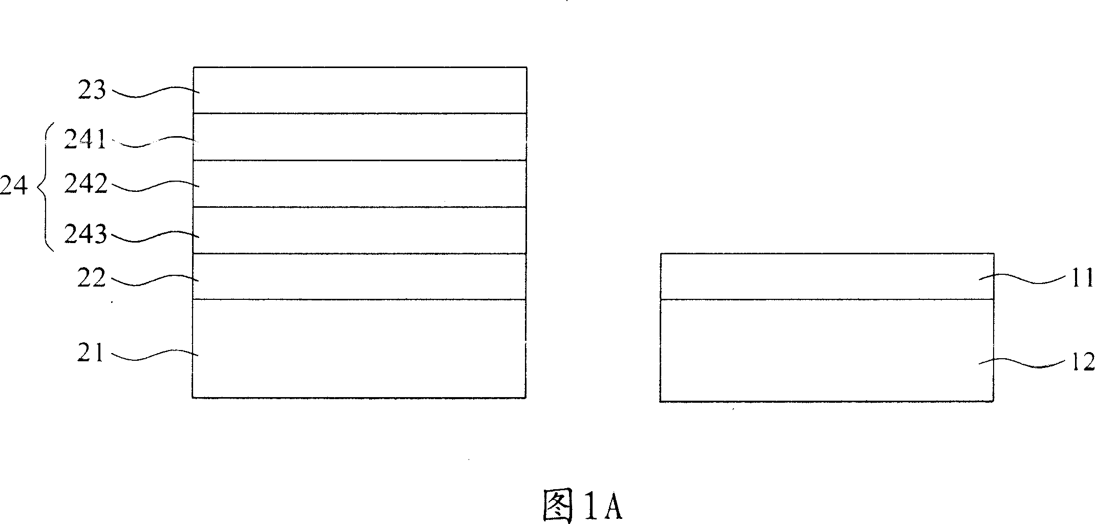
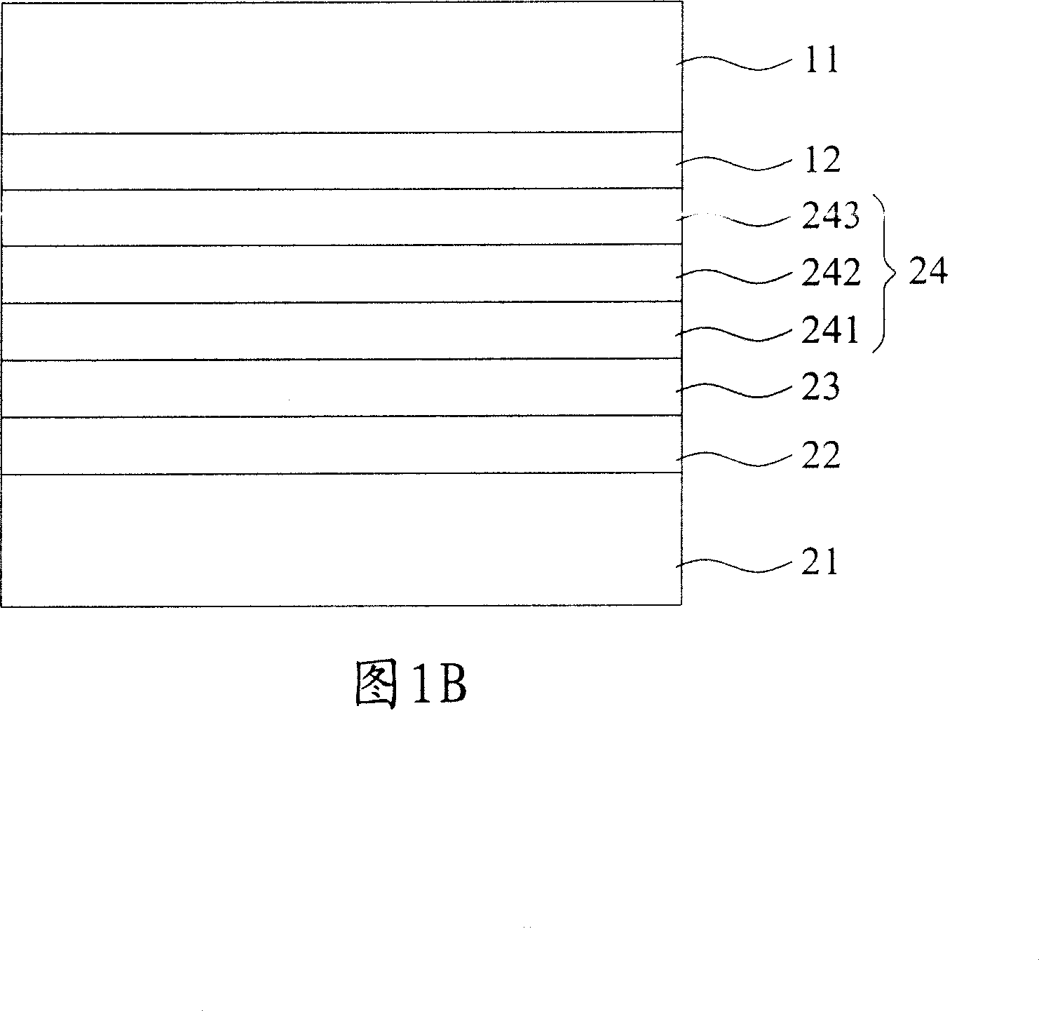
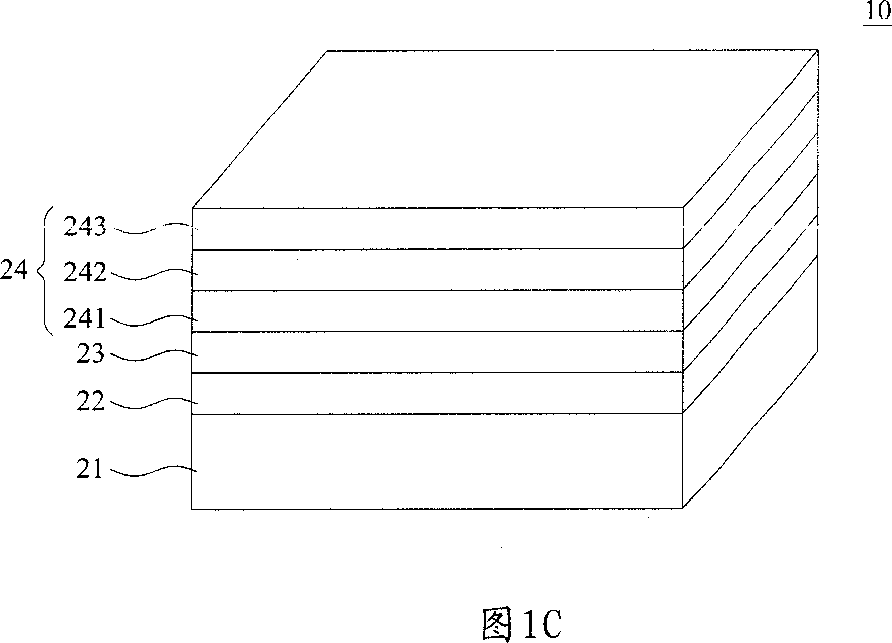
[0084] Please refer to FIG. 1A, FIG. 1B, and FIG. 1C. FIG. 1A is a schematic diagram of an embodiment in which a conventionally known first substrate 21 has not yet been combined with the light-emitting diode structure 10 in the previous process. FIG. 1B is a first substrate 21. A schematic diagram of an embodiment after being combined with the light-emitting diode structure 10 in the previous process. FIG. 1C is a perspective view of the embodiment after removing the temporary substrate 11 and the etch stop layer 12 in FIG. 1B .

[0085] Generally, the manufacture of the LED structure is to form the LED structure 10 of the pre-process that has not been divided into units and has not yet completed other insulating layers and conductive plates on a wafer in a semiconductor manufacturing process. However, when the actual light-emitting diode structure is applied, because the wafer is too thick and opaque, it cannot be applied and must be removed. Therefore, the wafer is only a t...

no. 2 example

[0106] 7 to 9B, this embodiment is a light emitting diode structure 30, which includes: a first substrate 21, an adhesive layer 22, at least two first ohmic connection layers 23', at least two epitaxial crystal layer 24 , a second insulating layer 31 , at least two fifth conductive plates 32 and at least two sixth conductive plates 33 .

[0107] The LED structure 30 of this example can be combined with the first substrate 21 coated with the adhesive layer 22 and the pre-process LED 28 formed on the wafer by using a process similar to that of FIG. 1A to FIG. 1C in the first embodiment. Then, the temporary substrate 11 and the etch stop layer 12 are removed by etching to obtain the light emitting diode structure 30 that has not been divided into units.

[0108] The above-mentioned first substrate 21 has a first surface 211 and a second surface 212 , and the first substrate 21 is mainly used to support the entire LED structure 30 . The first substrate 21 can be a single crystal,...


PUM


Abstract

The invention relates to a light-emitting diode structure which comprises a first substrate, an adhesive layer formed on the first substrate, a first ohmic connection layer formed on the adhesive layer, an epitaxial layer formed on the first ohmic connection layer, a first insulating layer covered on the exposed surfaces of the first ohmic connection layer and the epitaxial layer, a first current-conducting plate and a second current-conducting plate both formed inside the first insulating layer and electrically connected with the one end of the first ohmic connection layer and the epitaxial layer. With the arrangement of a first groove and a second groove, the complicated series / parallel circuit connection of the light-emitting diode structure can be performed conveniently, and thus the light-emitting diode structure, in a monomer form, is adapted to various operations in high pressure environment.

Description

technical field [0001] The invention relates to a light emitting diode structure, in particular to a high power light emitting diode structure applied in a high voltage environment. Background technique [0002] US Patent No. 6,853,011 discloses a light-emitting epitaxial layer structure, one end of which contains a light-absorbing temporary substrate, and the other end is adhered to a light-transmitting transparent substrate by phencyclobutene. Portions of the light-absorbing temporary substrate are then removed. Then, a connection channel is formed in the LED structure to connect the first ohmic contact electrode, and an insulating trench is formed to separate the active layer of the LED structure into two parts. Then, a second ohmic contact electrode is formed on the cladding layer, a bonding metal layer is filled in the first channel and successfully formed on the second ohmic contact electrode. Since the two bonding metal layers have the same height, the resulting LED...

Claims


Application Information

Patent Timeline
Patent Type & Authority Applications(China)
IPC IPC(8): H01L27/15H01L33/00H01L33/20
Inventor 许世昌陈明鸿温士逸
Owner HELIO OPTOELECTRONICS
Why Eureka
Try Eureka