Liquid crystal display device with color film on thin-film transistor and its manufacture method

A thin-film transistor and liquid crystal display technology, which is applied in semiconductor/solid-state device manufacturing, instruments, electrical components, etc., can solve the problems of disconnection of color film lithography process, decrease of pixel aperture ratio, decrease of light transmittance and aperture ratio, etc. , to achieve the effect of eliminating poor light leakage and other defects, reducing process steps and improving product yield

Active Publication Date: 2008-03-26
BEIJING BOE OPTOELECTRONCIS TECH CO LTD +1
View PDF3 Cites 37 Cited by
  • Summary
  • Abstract
  • Description
  • Claims
  • Application Information

AI Technical Summary

Problems solved by technology

There are still some shortcomings in the device structure or manufacturing method of the above invention: five photolithography processes are required to manufacture thin film transistors; the gate insulating film and passivation protective film cover the color filter layer, resulting in a decrease in light transmittance and aperture ratio; The removal of the matrix increases the critical size of the metal line and reduces the aperture ratio of the pixel; making two layers of pixel electrodes increases the complexity of the process; the difference in the accuracy of the color film photolithography process may lead to the disconnection of the two layers of pixel electrodes

Method used


Image

  • Liquid crystal display device with color film on thin-film transistor and its manufacture method
  • Liquid crystal display device with color film on thin-film transistor and its manufacture method
  • Liquid crystal display device with color film on thin-film transistor and its manufacture method

Examples


Embodiment Construction

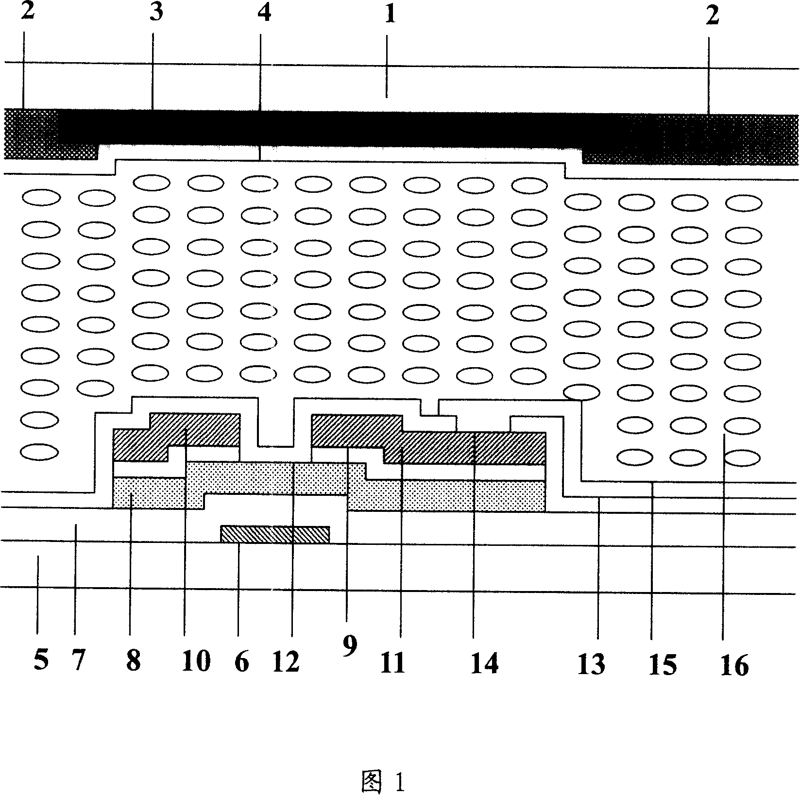
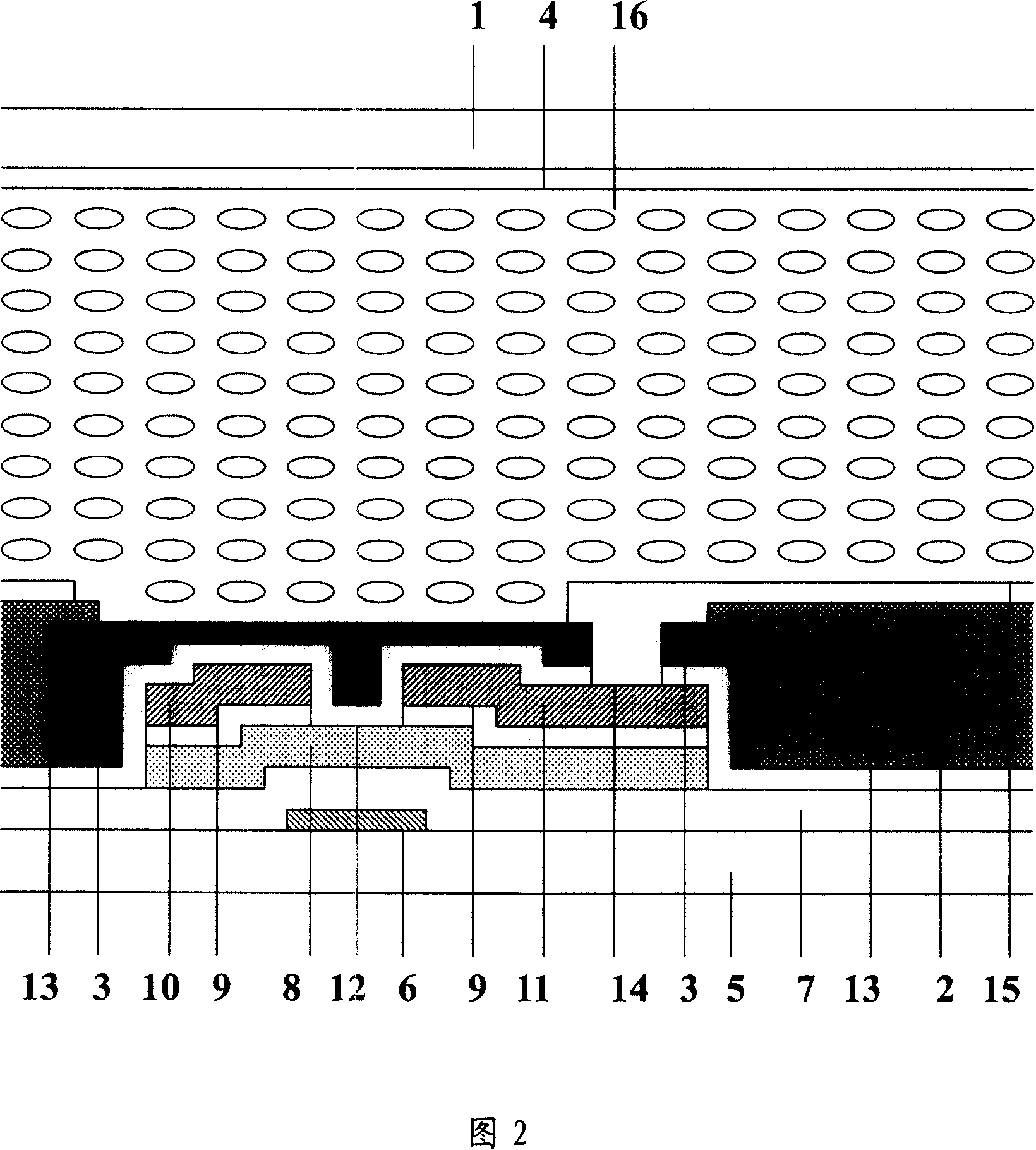
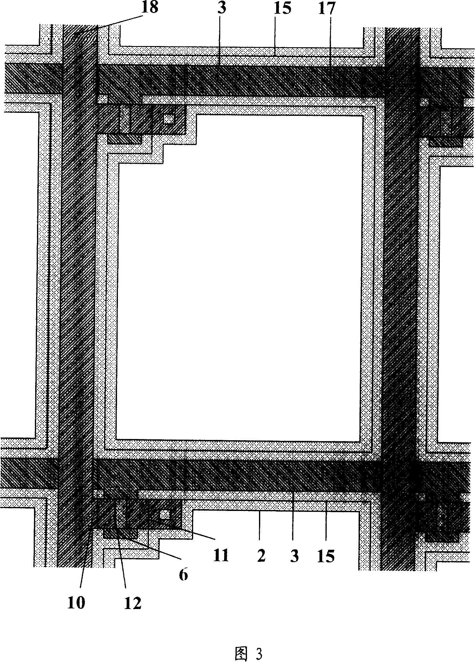
[0047] Specific embodiments of the present invention will be described in detail below in conjunction with the accompanying drawings. It should be pointed out that the film thicknesses and area sizes of the various layers in the drawings do not reflect the real scale of the device structure, but are only for clearly illustrating the content of the present invention.

[0048] The liquid crystal display device of the present invention comprises an array substrate and a common electrode substrate, liquid crystal molecules sandwiched between them, peripheral circuits and driving circuit boards, and a backlight source. The difference from traditional liquid crystal display devices is that the color filter layer and black matrix are formed on the thin film transistor, and the thin film transistor is formed on the glass of the array substrate; the other glass substrate only has a common electrode composed of a transparent conductive film. Figure 2 is a schematic cross-sectional view ...


PUM

PropertyMeasurementUnit
thicknessaaaaaaaaaa
thicknessaaaaaaaaaa
thicknessaaaaaaaaaa

Abstract

This invention discloses a sort of liquid crystal display that the chromatic film is above the thin film transistor, and it consists of the nether baseboard, the grating line, the grating pole, the thin film transistor is formed above the grating pole, the data wire, the power pole which connects with the data wire and the corresponding leakage pole are formed above the thin film transistor, the deactivation protective foil is formed above the channel of the thin film transistor, and it has the bore in the part which is corresponds to the leakage pole, the black matrix is formed above the deactivation protective foil, and it has the bore in that bore position, the hatch of the black matrix corresponds to the picture element area, the chromatic filter layer is formed in the hatch of the black matrix, a picture element pole is formed above the chromatic filter layer, and it connects with the leakage pole by the bore, the upper baseboard, the common pole which is formed above the nether baseboard, a liquid molecule layer is formed between the upper baseboard and the nether baseboard. This invention discloses the manufacturing method of this crystal display at the same time. This invention advances the penetrant rate and the hatch rate of the liquid crystal display, and it predigests the technique.

Description

technical field [0001] The invention relates to a liquid crystal display device and a manufacturing method thereof, in particular to a liquid crystal display device with a color filter on a thin film transistor and a manufacturing method thereof. Background technique [0002] Due to the advantages of thinness and low power consumption, flat panel displays are widely used in portable displays. Among various flat panel displays, liquid crystal display devices have been widely used in computer monitors, notebook computers and televisions due to their advantages of high definition and picture quality. The image display of liquid crystal display is realized by utilizing the optical anisotropy and polarization characteristics of liquid crystal molecules. These characteristics of the liquid crystal molecules themselves cause their different alignments to change the refraction and transmission of incident light. Because of the anisotropic dielectric properties of liquid crystal mo...

Claims


Application Information

Patent Timeline
Patent Type & Authority Applications(China)
IPC IPC(8): G02F1/136G02F1/1335G02F1/1333G03F7/20H01L21/00
Inventor 龙春平
Owner BEIJING BOE OPTOELECTRONCIS TECH CO LTD
Why Eureka
Try Eureka