Photon crystal filter with high distinguishability

A photonic crystal, high-resolution technology, applied in light guides, optics, instruments, etc., can solve the problems of low resolution, loss of photonic crystal plate, etc., and achieve the effect of improving filtering efficiency

Inactive Publication Date: 2008-04-16
INST OF PHYSICS - CHINESE ACAD OF SCI
View PDF0 Cites 8 Cited by
  • Summary
  • Abstract
  • Description
  • Claims
  • Application Information

AI Technical Summary

Problems solved by technology

However, optimizing the distance between the resonant cavity and the heterojunction interface is a very complicated work, and this optimization is very important for realizing the feedback effect, and in practical applications, a curved waveguide must also be introduced, and this curved waveguide will Introduces rather severe losses in two-dimensional photonic crystal slabs
Another example is the technology disclosed by the Notomi group in Document 3: "A.Shinya, S.Mitsugi, E.Kuramochi, and M.Notomi, Opt.Express 13, 4202 (2005)." It is proposed to use the width of the waveguide as a feedback way, but the technology still has the disadvantage of too low resolution

Method used


Image

  • Photon crystal filter with high distinguishability
  • Photon crystal filter with high distinguishability
  • Photon crystal filter with high distinguishability

Examples


Embodiment Construction

[0033] Below in conjunction with accompanying drawing and specific embodiment the present invention is described in further detail:

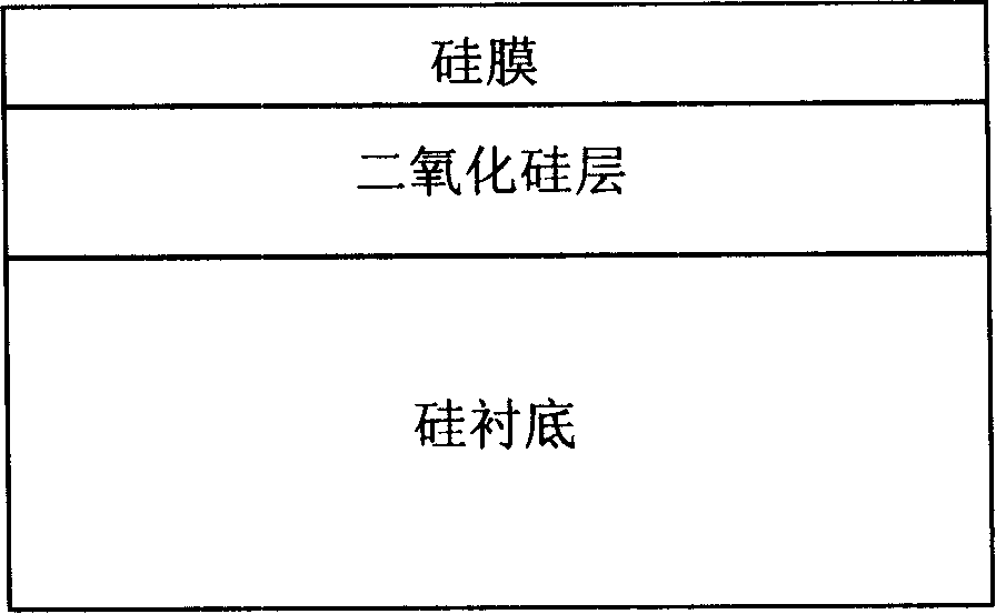
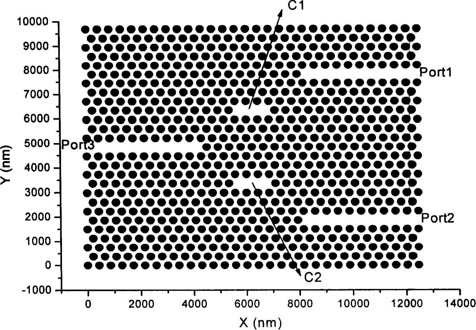
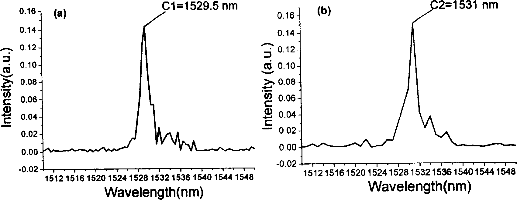
[0034] Such as figure 1 As shown, this embodiment takes a two-dimensional flat photonic crystal filter as an example to illustrate the present invention. In this embodiment, for example, an electron beam exposure system is used to process a photonic crystal device on a SOI (English full name is Silicon on Insulator, SOI for short) substrate. The thickness of the silicon film of the SOI sample is, for example, 235 nanometers, and the thickness of the buried layer of silicon dioxide is, for example, 375 nanometers. , the bottom layer is a silicon substrate, and the total thickness of the entire substrate is 0.5 mm. Using such as photoresist PMMA495 as an etching mask, this photoresist has good exposure characteristics and resolution, using the Raith150 electron beam exposure system produced by the German Raith company to define the photonic cryst...


PUM


Abstract

The invention discloses a photon crystal filter with high resolution, comprises a photon crystal, and is characterized in that: the photon crystal filter also comprises an input waveguide formed on the photon crystal, a first output waveguide and a second output waveguide; the input waveguide, the first output waveguide and the second output waveguide are respectively provided with a sealed end. Two point defect cavities are provided between the first and the second output waveguides and the input waveguide, The peaks of photon crystals at the two ends of the first point defect cavity respectively moves outward for a first distance; and the peaks of photon crystals at the two ends of the second point defect cavity respectively moves outward for a second distance; the second distance is larger than the first distance. The invention enhances filtering efficiency, and can realize fine filtering, therefore, the invention is more suitable for optical integrating systems with high density.

Description

technical field [0001] The invention relates to photonic crystal filter technology, in particular to a high-resolution photonic crystal filter capable of realizing nanoscale wavelength resolution. Background technique [0002] The two-dimensional photonic crystal plate has an in-plane photonic crystal band gap, and it is relatively easy to manufacture by using the current micromachining technology. Therefore, by introducing various artificial defects, a variety of optical devices can be realized, such as photonic crystal waveguides, resonant cavities , end-to-coupler and photonic crystal filter etc. As a current research hotspot, photonic crystal filters can be widely used in many fields, such as photonic integrated pathways, communications and quantum information processing. In the known technology, many different types of photonic crystal filters are designed and manufactured by researchers, such as Noda group in literature 1: "A.Chutinan, M.Mochizuki, M.Imada, and S.Noda...

Claims


Application Information

Patent Timeline
Patent Type & Authority Applications(China)
IPC IPC(8): G02B6/28G02B6/122
Inventor 任承陶海华刘娅钊李志远程丙英张道中
Owner INST OF PHYSICS - CHINESE ACAD OF SCI
Why Eureka
Try Eureka