Suspended structure subwavelength guided mode resonant terahertz high efficiency narrowband filtering method
A technology of guided mode resonance and suspended structure, which is applied to waveguide devices, optical filters, electrical components, etc., can solve the problems of low filtering efficiency and wide bandwidth, improve quality factor, overcome device asymmetry, and reduce loss Effect
- Summary
- Abstract
- Description
- Claims
- Application Information
AI Technical Summary
Problems solved by technology
Method used
Image
Examples
Embodiment 1
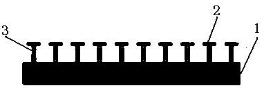
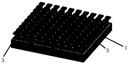
[0032] according to figure 1 , figure 2 As shown, the filter device of the present invention is mainly composed of a substrate 1, a terahertz resonant structure 2 and a support 3 of a suspended structure to form a two-dimensional umbrella array structure; wherein,
[0033] The substrate 1 is a high-resistance silicon substrate, polymethyl methacrylate or polyimide;
[0034] The patterned film structure 2 is made of high-resistance silicon, polymethyl methacrylate or polyimide material, and its shape is selected from geometric figures such as circle, star, square, etc., which can obtain a high resonance quality factor ;
[0035] The support structure 3 is made of silicon dioxide material.
Embodiment 2
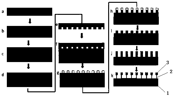
[0037] according to image 3 As shown, the filter device preparation process of the present invention includes the following steps:
[0038] 1. Deposit a silicon dioxide layer b on the high-resistance silicon substrate a by using a chemical vapor deposition process;
[0039] 2. Using a plasma sputtering process to sputter high-resistance silicon on the silicon dioxide layer b to form a high-resistance silicon film c;
[0040] 3. Spin-coating nano-imprint photoresist d on the high-resistance silicon film c by using a photoresist spin-coating process;
[0041] 4. Using nanoimprint template manufacturing technology to prepare nanoimprint template e according to filter device design requirements;
[0042] 5. Nanoimprint lamination f;
[0043] 6. The structure g obtained by separating the nanoimprint template e from the high-resistance silicon film c;
[0044] 7. The structure i obtained by removing the imprint photoresist after reactive ion etching of high-resistance silicon b...
PUM
 Abstract
Description
Claims
Application Information


