Chip embedding bury type packaging structure

A packaging structure and chip technology, applied in electrical components, electrical solid devices, circuits, etc., can solve the problems of chip cracking, ineffective heat dissipation, increased weight and cost, and achieve the effect of improving reliability.

Active Publication Date: 2008-05-14
PHOENIX PRECISION TECH CORP
View PDF0 Cites 11 Cited by
  • Summary
  • Abstract
  • Description
  • Claims
  • Application Information

AI Technical Summary

Problems solved by technology

[0007] Although the packaging structure of the chip embedded in the substrate can solve the above-mentioned defects of the prior art, however, due to the large difference in the coefficient of thermal expansion (Coefficient of Thermal Expansion, CTE) of the heat dissipation plate 12 and the insulating layer 14, the substrate structure in the manufacturing process is difficult. When the temperature changes (such as substrate baking (Baking), subsequent thermal cycle (Thermal Cycle) operations and other environments, different thermal stresses (Thermal Stress) are generated on each component), which is easy to cause the structure to warp (Warpage) phenomenon In severe cases, it may cause delamination between the structural layers, and even squeeze the semiconductor chip, causing the chip to break
However, increasing the thickness of the heat dissipation plate to balance the thermal stress on the substrate during temperature changes can effectively improve the substrate warpage phenomenon, but increasing the thickness of the heat dissipation plate will significantly increase the volume and thickness of the finished package structure, and will result in cost of the manufacturing method increase
[0008] In addition, most of the semiconductor chips embedded in the above packaging structure are of a single form and the same size, and have not yet formed a multi-functional module structure, which does not conform to the current development trend of electronic products.
In addition, if a variety of semiconductor components with different sizes are embedded in the package structure to achieve a multifunctional module structure, the electrical connection surfaces of these components are not in the same position due to the different sizes of the embedded components. The surface of the insulating layer on the surface of the packaging substrate where these components are embedded is uneven, and even affects the manufacturing quality of subsequent fine lines on the insulating layer
[0009] Therefore, how to propose a chip-embedded packaging structure to overcome the warping of the structure during the manufacturing process of the existing semiconductor packaging structure, the increase in the thickness, weight and cost of the packaging structure, the uneven manufacturing surface, the inability to improve the ability of the circuit manufacturing method, and the interface Problems such as difficult integration and inability to effectively dissipate heat have become technical problems that need to be overcome urgently in this field

Method used


Image

  • Chip embedding bury type packaging structure
  • Chip embedding bury type packaging structure
  • Chip embedding bury type packaging structure

Examples


Embodiment Construction

[0050] Embodiments of the present invention are described below through specific specific examples, and those skilled in the art can easily understand other advantages and effects of the present invention from the content disclosed in this specification. The present invention can also be implemented or applied through other different specific embodiments, and various modifications and changes can be made to the details in this specification based on different viewpoints and applications without departing from the spirit of the present invention.

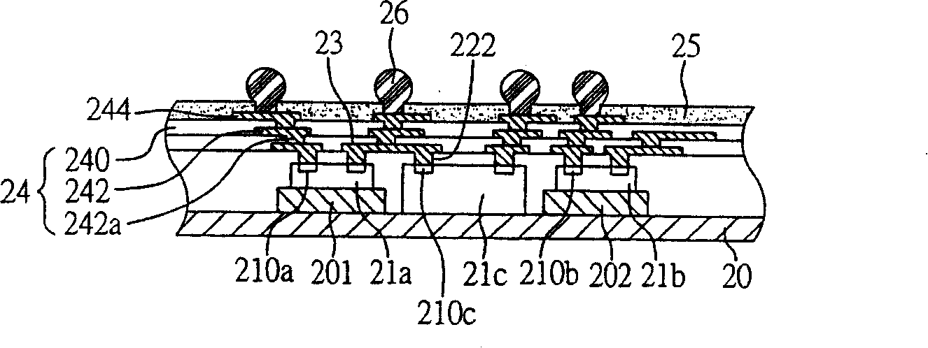
[0051] The chip-embedded package structure of the present invention is mainly characterized in that the carrier board has at least one raised portion for receiving a semiconductor chip. The protruding part is described in detail as an example, but it is not used to limit the present invention.

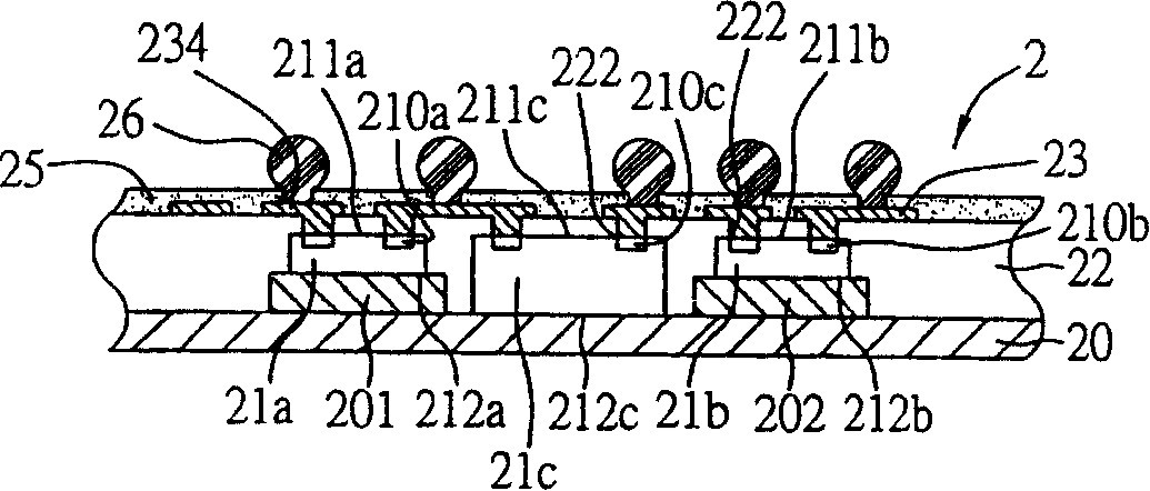
[0052] see Figure 2A , is a schematic cross-sectional view of a preferred embodiment of the chip-embedded package structure of the present...


PUM


Abstract

A chip-embedded encapsulation structure is provided, which consists essentially of a bearing board with a raised section, a semiconductor chip formed on the raised section of the bearing board, an insulation layer formed on the bearing board and the semiconductor chip, as well as a circuit layer formed on the insulated layer. The circuit layer can be electrically connected to an electrode cushionof the semiconductor chip through a plurality of conductive structures so that the semiconductor chip can electrically extend outwards. By adjusting the thicknesses of the raised section of the bearing board, the insulation layer and the bearing board, warping phenomenon of the encapsulation structure caused by changes of temperature during manufacture can be controlled.

Description

technical field [0001] The invention relates to a chip-embedded package structure, in particular to a package structure which embeds a semiconductor chip and makes it electrically extended outward. Background technique [0002] With the evolution of semiconductor packaging technology, different packaging forms have been developed for semiconductor devices. Traditional semiconductor devices mainly install a semiconductor component such as an integrated circuit on a package substrate or a lead frame, and then The semiconductor component is electrically connected to the packaging substrate or the lead frame, and then packaged with glue. Among them, Ball grid array (BGA) is an advanced semiconductor packaging technology, which is characterized in that a packaging substrate is used to place semiconductor components, and self-alignment technology is used to implant semiconductor components on the back of the packaging substrate. A plurality of solder balls (Solder ball) arranged ...

Claims


Application Information

Patent Timeline
Patent Type & Authority Applications(China)
IPC IPC(8): H01L25/00H01L23/48H01L23/52H01L23/367
CPCH01L24/19H01L2924/0002H01L2924/351H01L2224/12105H01L2224/24137H01L2224/32245H01L2224/73267H01L2224/92244H01L2924/15153H01L2924/14H01L2224/19H01L2924/00H01L2924/00012
Inventor 许诗滨
Owner PHOENIX PRECISION TECH CORP
Why Eureka
Try Eureka