Method of producing ZnO based transparent film transistor array

A technology of transistors and thin films, which is applied in the field of preparation of ZnO-based transparent thin film transistor arrays, can solve the problems of affecting the charge storage characteristics of liquid crystal pixels, improving the mobility of amorphous silicon thin film transistors, etc.

Inactive Publication Date: 2008-05-21
XI AN JIAOTONG UNIV
View PDF0 Cites 32 Cited by
  • Summary
  • Abstract
  • Description
  • Claims
  • Application Information

AI Technical Summary

Problems solved by technology

However, amorphous silicon thin film transistors have low mobility and strong photoelectric effect, which affect the charge storage characteristics of liquid crystal pixels.
The preparation process of polysilicon thin film transistors is complex and costly, and silicon-based thin film transistors are opaque in the visible light band, which limits the improvement of the aperture ratio of the display unit
However, organic semiconductor thin film transistors (OTFTs) are difficult to overcome the shortcomings of low lifespan and low mobility.

Method used


Image

  • Method of producing ZnO based transparent film transistor array
  • Method of producing ZnO based transparent film transistor array
  • Method of producing ZnO based transparent film transistor array

Examples


Embodiment 1

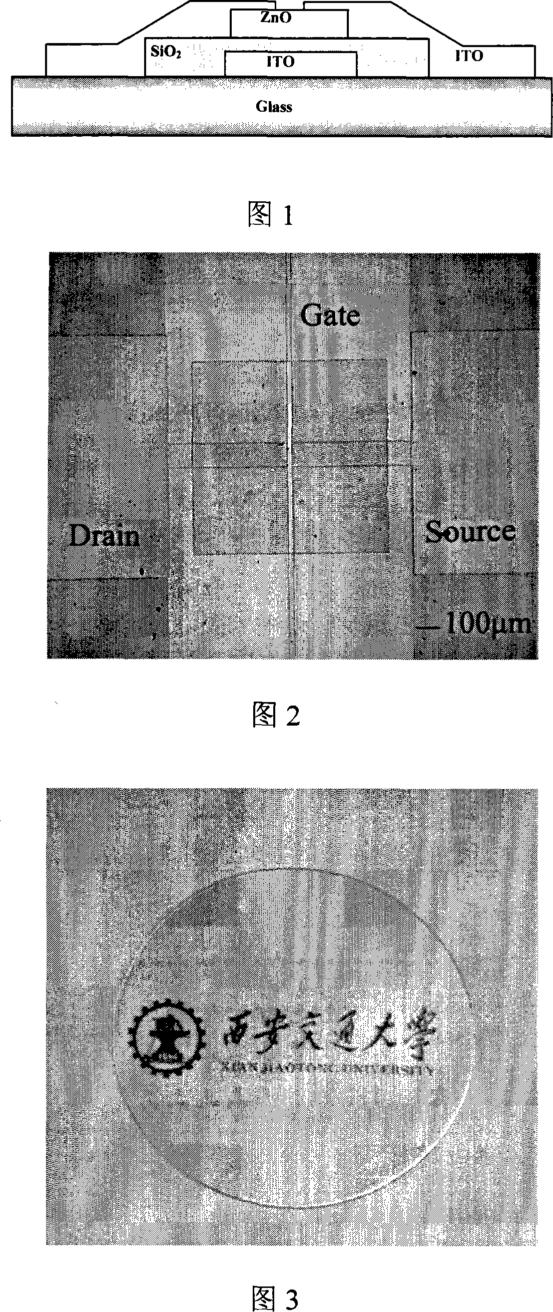
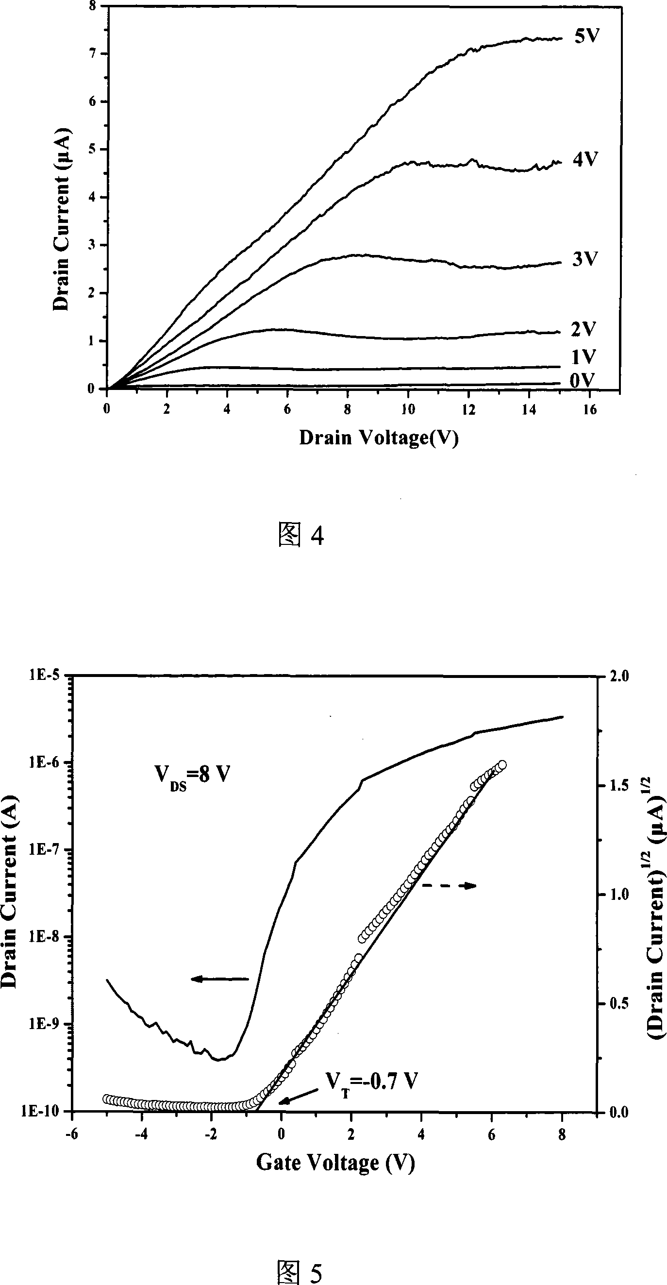
[0026] This embodiment is to prepare a ZnO channel layer transparent thin film transistor array, and the specific implementation steps are:

[0027] 1. Lithographically engrave the gate pattern on the ordinary glass or quartz substrate, then grow the ITO transparent conductive film by magnetron sputtering, take out the sample and ultrasonically in the acetone solution for several minutes to form the gate pattern, the thickness of the gate film is about 200nm;

[0028] 2. Overlay the insulating layer pattern on the ITO gate twice, and grow SiO by magnetron sputtering 2 The thin film is used as an insulating layer, and the excess photoresist is partially peeled off in acetone ultrasonically;

[0029] 3. Overlay the channel layer pattern on the insulating layer film, and grow the ZnO film by magnetron sputtering, and then remove the excess photoresist by ultrasonic in acetone;

[0030] 4. Anneal the sample in an oxygen atmosphere at 500°C for 1 hour;

[0031] 5. On the ZnO chan...

Embodiment 2

[0035] The difference between this example and Example 1 is that the ITO film in Step 1 and Step 5 is replaced by a transparent conductive film such as ZnO:Al or ZnO:Ga, and a transparent ZnO-TFT array can also be prepared.

Embodiment 3

[0037] The difference between this embodiment and embodiment 1 is that the SiO in step 2 2 Thin film replaced by HfO 2 、Al 2 o 3 or Y 2 o 3 Etc. transparent insulating layer film, other are all the same as embodiment 1.


PUM

PropertyMeasurementUnit
thicknessaaaaaaaaaa

Abstract

The invention discloses a method for preparing a transparent ZnO-based thin film transistor array. The method adopts a preparation process of four peeling processes, uses radio frequency magnetron sputtering technology to grow a ZnO-based thin film, and anneals the ZnO-based thin film in oxygen to obtain improve its electrical properties. The thin film transistor array uses transparent conductive films such as ITO, ZnO:Al or ZnO:Ga as gate, source and drain electrodes, and uses SiO2, Al2O3, SiNX and other films as insulating layers. The experiment shows that the transmittance of the ZnO-based thin film transistor array in the visible light band reaches 85%, which provides a new way for the development of high-performance flat panel display arrays.

Description

technical field [0001] The invention belongs to the technical field of flat panel display (FPD), and relates to a method for preparing a ZnO-based transparent thin-film transistor array. The ZnO-based transparent thin-film transistor array prepared by the method has a high transmittance in the visible light band, and is useful for developing a high-performance flat panel Display arrays offer a new avenue. Background technique [0002] With the advent of the information age, active-driven flat-panel display technology has become more and more widely used, the most typical representatives of which are thin-film transistor-driven liquid crystal displays (TFT-LCD) and thin-film transistor-driven organic light-emitting diode displays (TFT-OLED). As a switching element, transistor plays a vital role in improving the performance of display devices. In order to realize display devices with low power consumption, fast response speed, and stable process, thin-...

Claims


Application Information

Patent Timeline
Patent Type & Authority Applications(China)
IPC IPC(8): H01L21/84H01L21/336H01L21/477G02F1/1362
Inventor 张景文张新安侯洵张杰
Owner XI AN JIAOTONG UNIV
Why Eureka
Try Eureka