Wiring substrate and semiconductor device using the same

A technology for wiring substrates and semiconductors, which is applied in the fields of semiconductor devices, semiconductor/solid-state device manufacturing, and semiconductor/solid-state device components, etc., and can solve the problem of decreased productivity of semiconductor devices, deformation of wiring 5 for electroplating, difficulty in electrical inspection of semiconductor component substrates 1, etc. problems, to achieve the effect of improving productivity and improving reliability

Inactive Publication Date: 2008-05-28
PANASONIC CORP
View PDF1 Cites 13 Cited by
  • Summary
  • Abstract
  • Description
  • Claims
  • Application Information

AI Technical Summary

Problems solved by technology

[0011] In this way, if the wiring 5 for plating is exposed from the side of the semiconductor device, when it is mounted on a printed circuit board of an electronic device in a subsequent inspection process, the socket for inspection or a suction tool during mounting of a printed circuit board may come into contact with the wiring for plating. At this time, the wiring 5 for electroplating is often deformed and an electrical short circuit occurs between adjacent wiring 5 for electroplating.
In addition, due to the adhesion of impurity ions and the moisture absorption of the semiconductor device, the plating wiring 5 causes migration on the side surface.
Due to the above reasons, there is a problem that the reliability of semiconductor devices decreases
[0012] In addition, before cutting the wiring board 8 and the sealing resin 15 with the dividing line 9 to divide into each semiconductor device, almost all the internal wiring 3 is in a state of being electrically connected (short-circuited) by the wiring 5 for plating, so the 8, it is difficult to conduct an electrical inspection of each semiconductor component substrate 1, and semiconductor chips 13 may be mounted on unqualified semiconductor component substrates 1, and as a result, there is also a problem that the productivity of semiconductor devices decreases.

Method used


Image

  • Wiring substrate and semiconductor device using the same
  • Wiring substrate and semiconductor device using the same
  • Wiring substrate and semiconductor device using the same

Examples


Embodiment Construction

[0036] Next, a wiring board showing an embodiment of the present invention and a semiconductor device using the wiring board will be described in detail with reference to the drawings.

[0037] A wiring board according to an embodiment of the present invention will be described.

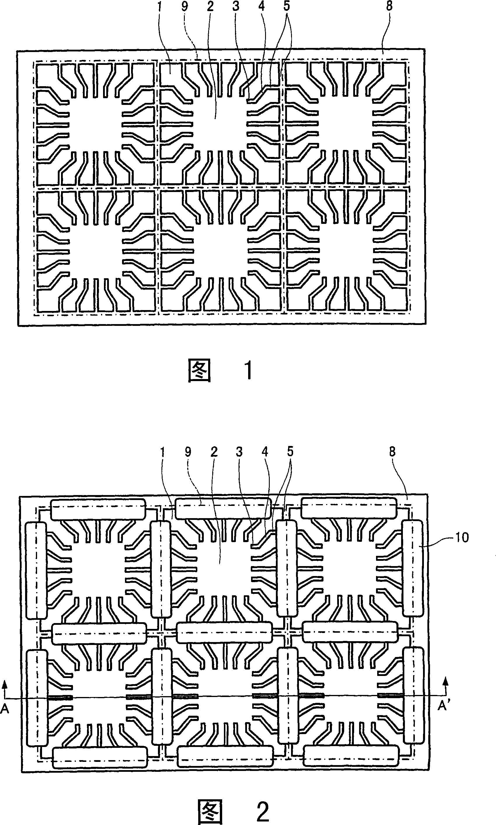
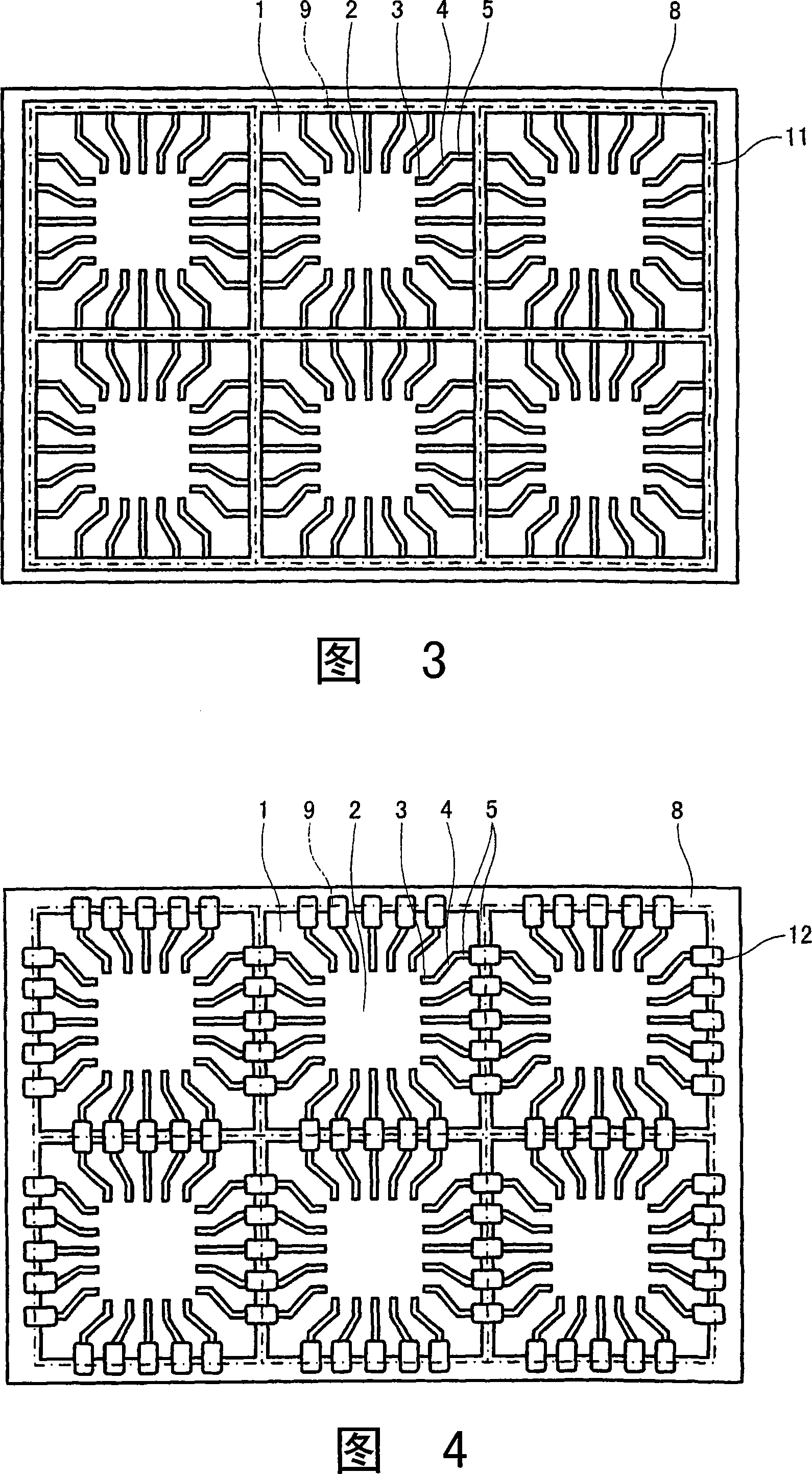
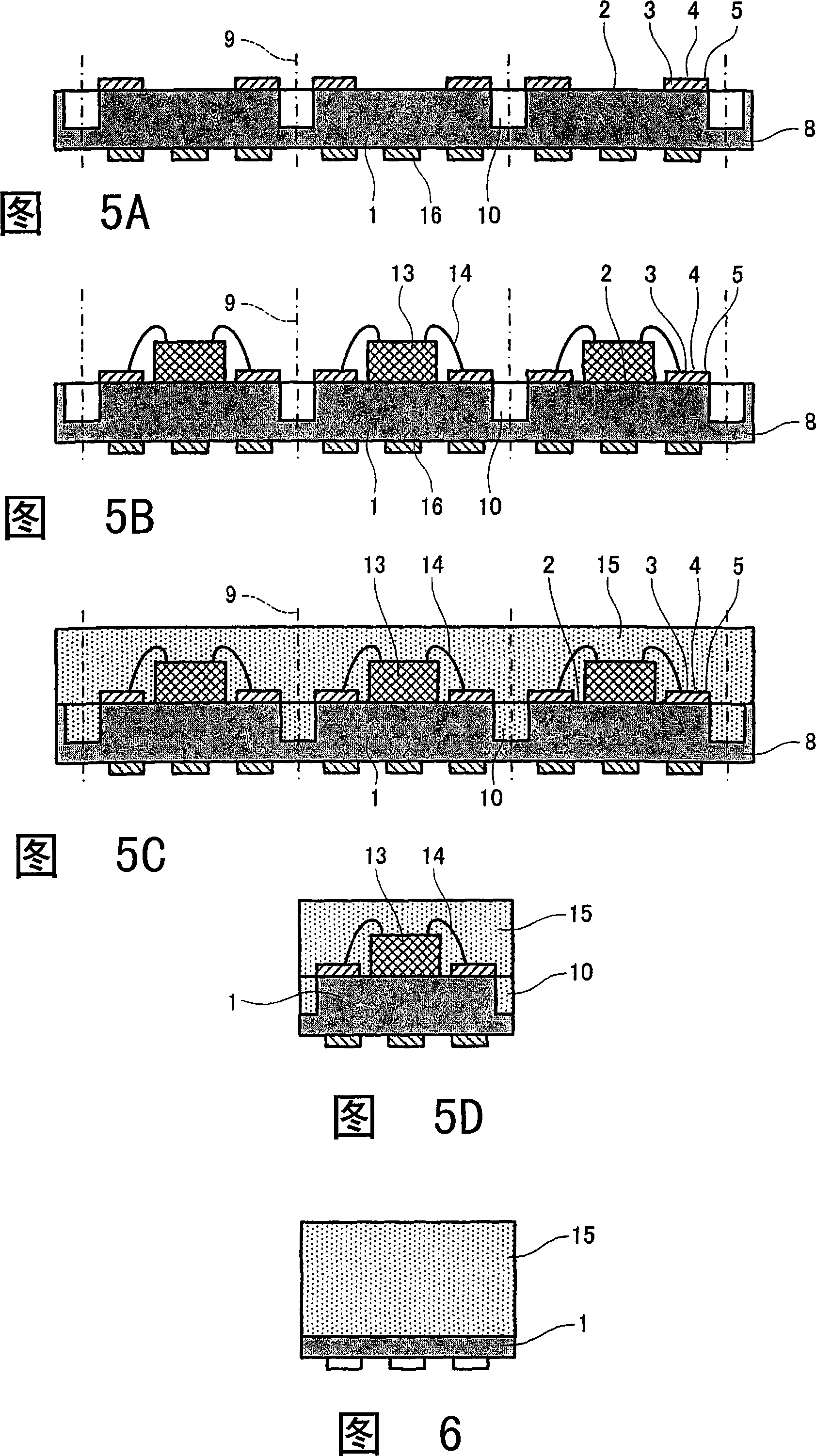
[0038] FIG. 1 is a plan view showing a state in which a wiring pattern is formed on a wiring substrate of this embodiment, and FIG. 2 is a diagram showing a groove-shaped concave portion formed only on the wiring portion for plating on the outer periphery of each semiconductor package substrate on the wiring substrate of this embodiment. FIG. 3 is a plan view showing a state in which an annular recess is formed over the entire outer periphery of each semiconductor module substrate on the wiring board of this embodiment. FIG. It is a plan view of a state where an independent recess is formed for each plating wiring on the outer periphery of each semiconductor module substrate.

[0039] First, in FIG....


PUM


Abstract

According to the present invention, a plurality of semiconductor devices having semiconductor chips 13 molded on a semiconductor package substrate 1 by a molding resin 15 can be manufactured by forming recesses 10 around each semiconductor package substrate 1 composing a substrate 8 for a BGA package, and in the state where a molding resin 15 is filled on the substrate 8 including the recesses 10 for resin molding, cutting the substrate 8 and the molding resin 15 along partition lines 9.

Description

technical field [0001] The present invention relates to a wiring substrate composed of a plurality of semiconductor module substrates on which semiconductor chips are mounted, used in, for example, a BAG package, and a semiconductor device using the wiring substrate. Background technique [0002] In recent years, in order to cope with the miniaturization of electronic equipment such as mobile communication equipment, miniaturization and high density are required even for semiconductor devices. In addition, with the development of high performance and multi-functionalization of electronic equipment, in semiconductor devices, external terminals tend to have multiple pins, and BAG components and LAG components arranged in arrays on the bottom surface of semiconductor components are mostly used. [0003] Such a semiconductor device is obtained by cutting the wiring substrate and sealing resin for each semiconductor module substrate in a state where a semiconductor chip is sealed...

Claims


Application Information

Patent Timeline
Patent Type & Authority Applications(China)
IPC IPC(8): H01L23/498H01L23/13H01L23/488H01L23/31
CPCH01L2224/45124H01L23/3121H01L2924/01082H05K3/284H01L2924/01004H01L2224/97H01L2224/48699H01L2924/01002H01L2924/15159H01L2924/20752H01L2924/01029H01L23/13H05K3/0052H01L2924/01028H01L2224/48091H01L2924/01013H01L2224/85447H01L2224/45147H01L2924/20751H01L24/97H01L2224/45015H01L2224/484H01L24/48H01L24/45H01L2224/48599H05K2201/0909H01L2924/01079H01L2224/48227H01L2924/01005H01L2924/01033H01L2924/01006H01L2924/01078H05K2201/09036H01L2224/45144H01L21/561H01L2224/48799H01L2924/181H01L2224/48847H01L2224/48647H01L2224/48747H01L2924/00014H01L2224/85H01L2924/00H01L2924/00012
Inventor 藤本博昭今津健一
Owner PANASONIC CORP
Why Eureka
Try Eureka