

Annealing method for producing large area two-side thallium series film
A large-area, annealing technology, applied in the direction of ion implantation plating, metal material coating process, coating, etc., can solve the problems of film surface shedding, uneven pattern, complex device, etc., achieve low cost, avoid pollution, improve Effect of Diffusion Velocity
- Summary
- Abstract
- Description
- Claims
- Application Information
AI Technical Summary
Problems solved by technology
Method used
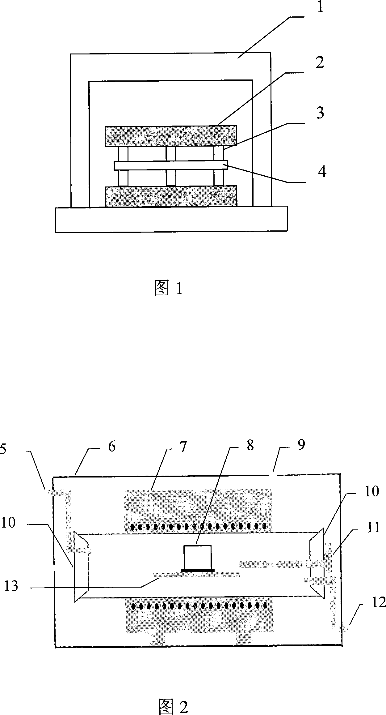
Image

Examples
Embodiment 1
[0028] The composition is Tl 2 Ba 2 CaCu 2 o 8 (m=2, n=2) Two-inch double-sided thallium-based high-temperature superconducting thin film. The used substrate and single crystal block materials are all lanthanum aluminate (001) oriented single crystals. The thickness of the substrate is 0.5 mm, and the thickness of the single crystal block is 1.5 mm. The annealing temperature is 730°C, and the precursor film is Ba with a thickness of 500nm without thallium. 2 CaCu 2 o Y Amorphous thin film, thallium source is Tl 2 Ba 2 Ca 2 Cu 3 o 10 blocks. The annealing time was 3 hours, and the argon gas flow rate was 25ml / min, and finally a sample with the same electrical properties of the superconducting thin film on both sides was obtained. This annealing process was repeated several times to prepare multiple samples. The superconducting critical temperature T of each sample was obtained by the conventional four-lead measurement method c All within 103-108.5K; the supercond...
Embodiment 2
[0030] The thallium source and precursor film with the same composition as in Example 1 are used, the wafer and single crystal block used are also lanthanum aluminate, the orientation is (001), the annealing temperature is 750°C, the thickness of the precursor film is 600nm, and the annealing time is 3.5 hours, the argon flow rate is 30ml / min, and finally obtain a sample with the same electrical properties of the superconducting film on both sides, and obtain the superconducting critical temperature T through the above-mentioned various measurement methods. c , superconducting critical current density J c (77K) and film microwave surface resistance R S (77K, 10GHz) are also in 103-108.5K, 1-3.0×10 6 A / cm 2 and less than 500µΩ range.
Embodiment 3
[0032] The thallium source and precursor film of the same composition as in Example 1 are adopted, the used wafer and single crystal block are all strontium titanate, the orientation is (001), the annealing temperature is 730 ° C, the thickness of the precursor film is 500 nm, and the annealing time is 3 hours, the argon flow rate is 25ml / min, and finally a superconducting sample with consistent electrical properties on both sides of the film is obtained. The superconducting critical temperature T is measured by the above-mentioned various measurement methods. c , superconducting critical current density J c (77K) and film microwave surface resistance R S (77K, 10GHz) are also in 103-108.5K, 1-3.0×10 6 A / cm 2 and less than 500µΩ range.
PUM
| Property | Measurement | Unit |
|---|---|---|
| thickness | aaaaa | aaaaa |
| diameter | aaaaa | aaaaa |
| thickness | aaaaa | aaaaa |
Abstract
Description
Claims
Application Information