Method and device for controlling wafer DC auto-bias and compensating electrostatic gravitational force between direct current electrode and water

A technology of DC electrodes and electrostatic attraction, which is applied in the manufacture of circuits, electrical components, semiconductors/solid-state devices, etc., can solve problems such as inaccuracy, signal loss changes, and cannot be determined or estimated in advance, so as to improve process results and reduce Effect of Small Helium Leak Rates

Inactive Publication Date: 2008-07-02
BEIJING NAURA MICROELECTRONICS EQUIP CO LTD
View PDF0 Cites 17 Cited by
  • Summary
  • Abstract
  • Description
  • Claims
  • Application Information

AI Technical Summary

Problems solved by technology

However, it has been found through experiments that although the DC self-bias voltage of the wafer is mainly generated by the RF signal loaded on the lower electrode, it is also affected by other process parameters. Therefore, when the process conditions change, the above passing rules will be becomes less accurate, and thus also loses accuracy in the measurement of wafer DC self-bias
[0010] In summary, the existing technical solutions have the following defects in controlling and compensating the DC self-bias voltage of the wafer. Due to the change of process conditions, there are certain difficulties in accurately measuring the DC self-bias voltage of

Method used


Image

  • Method and device for controlling wafer DC auto-bias and compensating electrostatic gravitational force between direct current electrode and water
  • Method and device for controlling wafer DC auto-bias and compensating electrostatic gravitational force between direct current electrode and water
  • Method and device for controlling wafer DC auto-bias and compensating electrostatic gravitational force between direct current electrode and water

Examples


Embodiment Construction

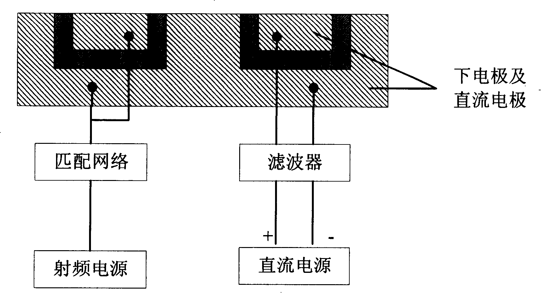
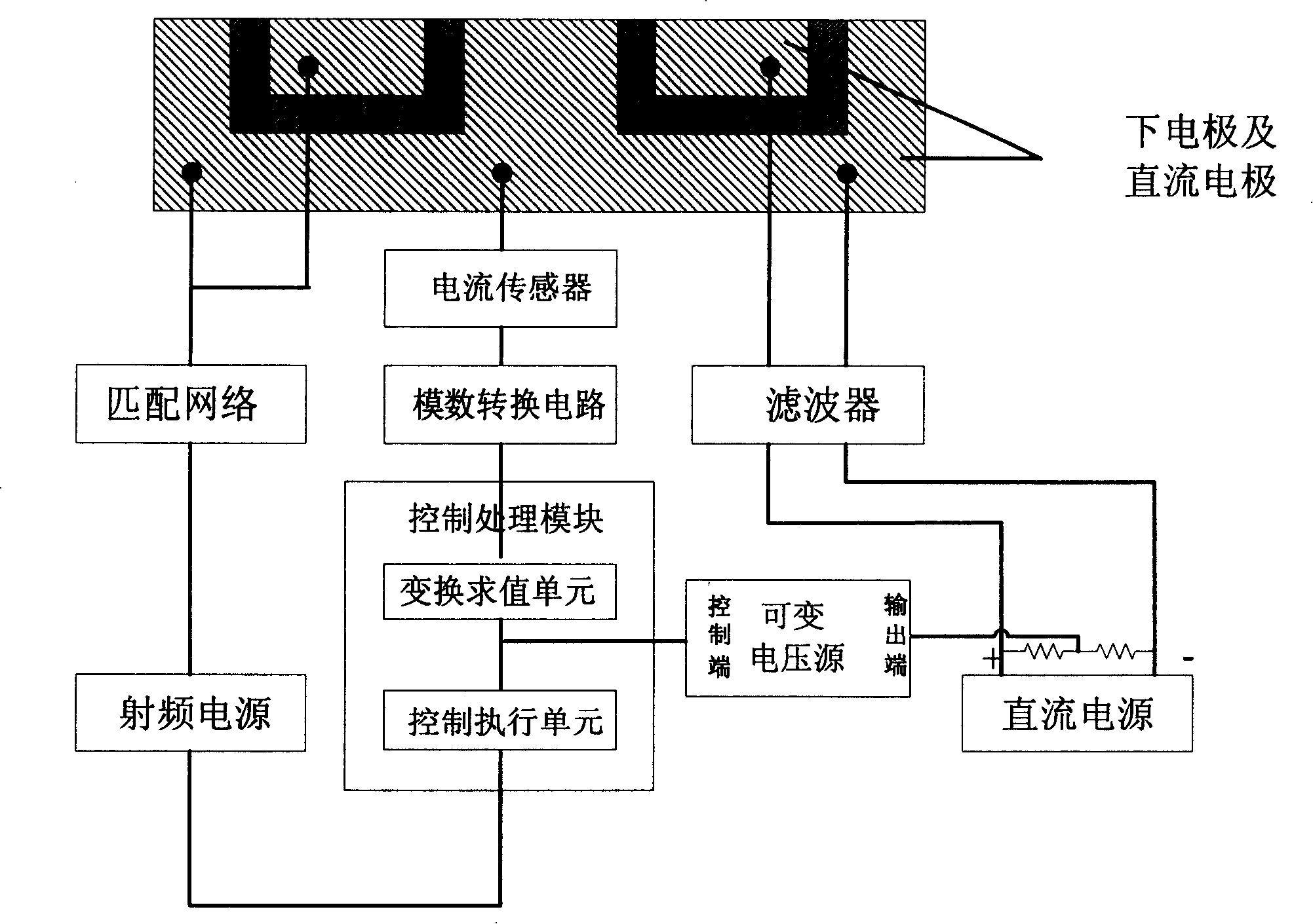
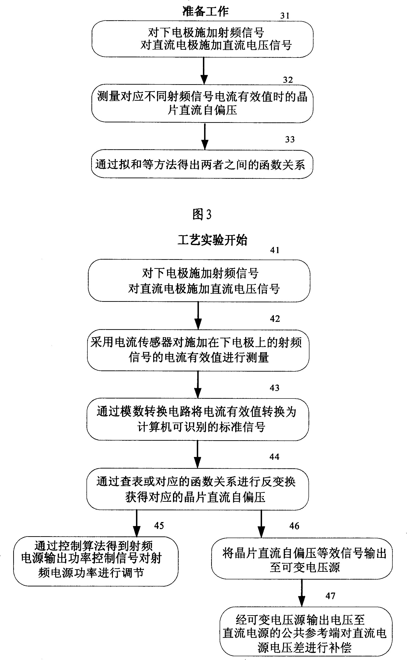
[0056] The present invention controls and compensates the DC self-bias voltage of the wafer by constructing a closed-loop feedback system, that is, indirectly obtains the value of the DC self-bias voltage by measuring a parameter that can characterize the magnitude of the DC self-bias voltage of the wafer, and then controls or compensates the value of the DC self-bias voltage The conversion links are respectively used to control the common reference terminals of the radio frequency power supply and the DC power supply. These include:

[0057] 1. The implementation method of controlling the DC self-bias voltage of the chip, including:

[0058] Measure a parameter that can characterize the DC self-bias voltage of the chip to indirectly obtain the value of the DC self-bias voltage, and then output the control signal after the value is compared and controlled to control the output power of the RF power supply, and then realize the control of the chip. DC self-bias control. in: ...


PUM


Abstract

The invention relates to a method for controlling the DC self-bias voltage of a wafer, a device, a method for complementing the electrostatic force between a DC electrode and the wafer and a device. The invention comprises the following steps: the value of the DC self-bias voltage is indirectly obtained by detecting a parameter which can characterize the value of the DC self-bias voltage and then the value of the DC self-bias voltage is respectively used for the control of an RF power supply and the public reference junction of a DC power supply after links of control or conversion so as to reach the goal of stably controlling the DC self-bias voltage on the wafer and complementing the imbalance of the electrostatic force between the wafer and the DC electrode caused by the DC self-bias voltage, so the realization of the invention on one hand can stably control the DC self-bias voltage on the wafer to obtain the process parameters such as the good etching rate, the deposition rate, etc., on the other hand can automatically complement the imbalance of the electrostatic force between two DC electrodes and the wafer caused by the self-bias voltage of the wafer to ensure that an electrostatic chuck can be better attached to the wafe so as to reduce the leak rate of the helium and improve the process result.

Description

technical field [0001] The invention relates to the technical field of automatic control, in particular to a method and device for controlling the DC self-bias voltage of a chip, and a method and device for compensating the electrostatic attraction between a DC electrode and the chip. Background technique [0002] With the development of microelectronics technology, plasma etching technology is widely used in the manufacturing process of semiconductor devices. The working principle of plasma etching equipment is as follows: [0003] Plasma contains a large number of active particles, such as electrons, positive ions, excited atoms, molecules and free radicals. Since electrons are lighter than positive ions, the number of electrons falling on the surface of the wafer is less than that of There are many ions, and after they stabilize, a DC negative bias voltage will be formed on the wafer surface. Then, this DC negative bias will attract positively charged ions and active rea...

Claims


Application Information

Patent Timeline
IPC IPC(8): H01L21/00H01L21/3065C23F4/00H05H1/02
Inventor 赵祎
Owner BEIJING NAURA MICROELECTRONICS EQUIP CO LTD
Why Eureka
Try Eureka