A method of manufacturing a mems element

A technology of components and micro-electromechanical components, which is applied in the field of manufacturing electronic devices, can solve the problem of difficulty in controlling the removal of sacrificial layers

Inactive Publication Date: 2008-07-02
KONINKLIJKE PHILIPS ELECTRONICS NV
View PDF6 Cites 21 Cited by
  • Summary
  • Abstract
  • Description
  • Claims
  • Application Information

AI Technical Summary

Problems solved by technology

[0006] A disadvantage of existing devices and existing methods is

Method used


Image

  • A method of manufacturing a mems element
  • A method of manufacturing a mems element
  • A method of manufacturing a mems element

Examples


Embodiment Construction

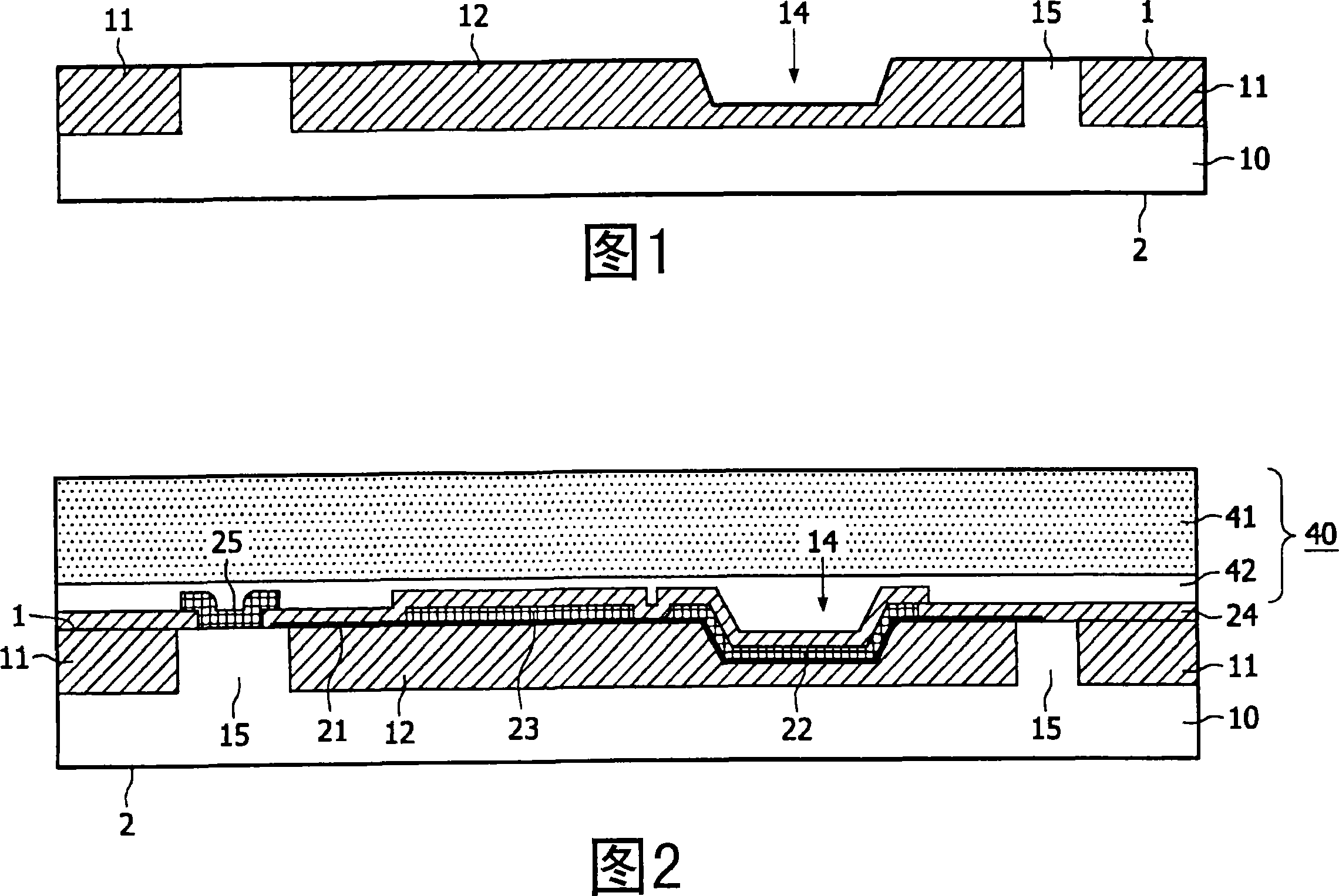
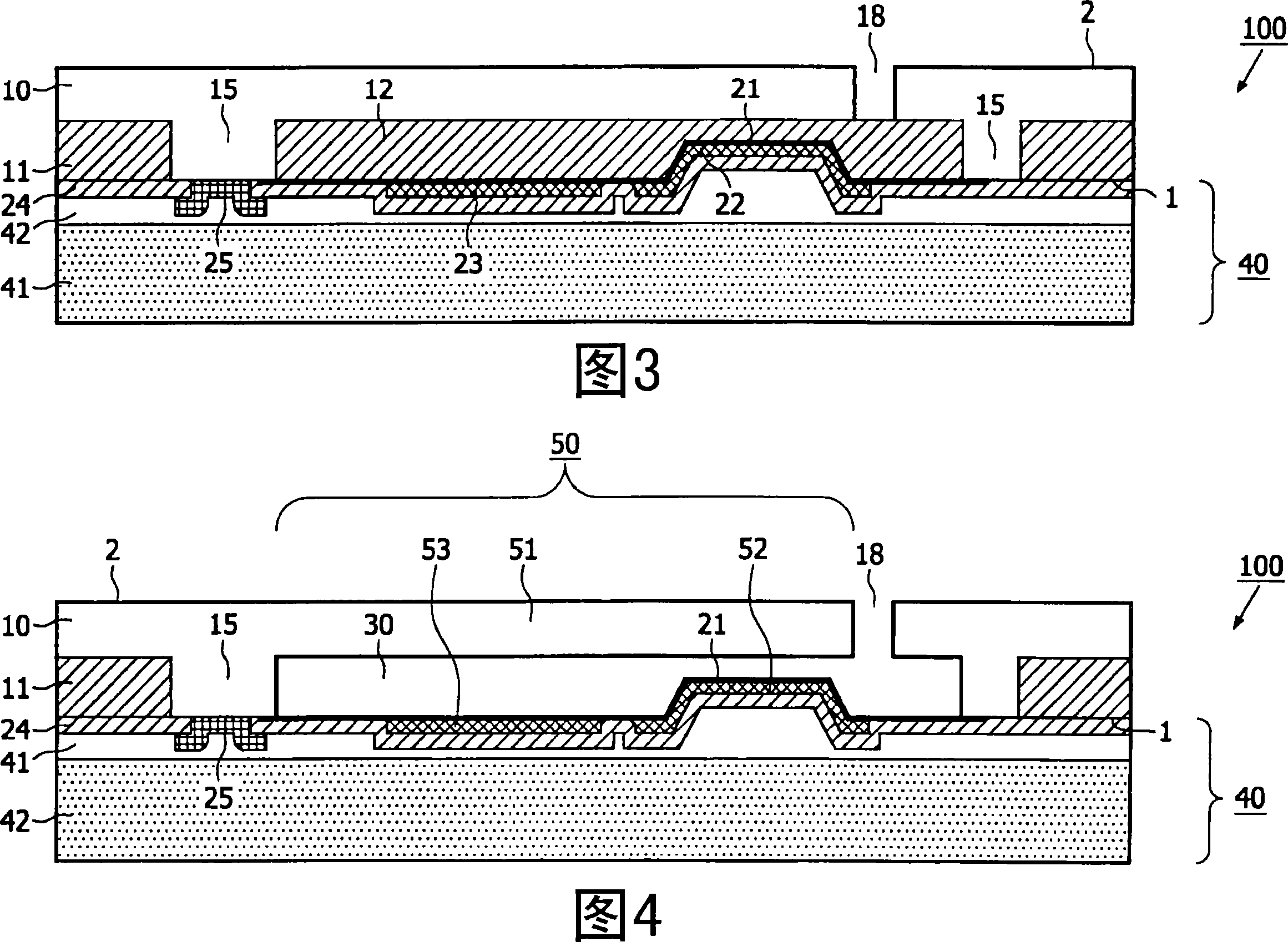
[0043] 1-4 show a first embodiment of the method of the invention in cross-sectional view.

[0044] FIG. 1 shows a substrate 10 having a first surface 1 , and a second surface 2 . In this case, the substrate 10 is a silicon substrate, which is doped n-type or p-type so as to be sufficiently conductive. The dopants extend in particular to a depth of 10-20 microns. On the first surface 1 , the substrate 10 has been locally oxidized and at least one pillar 15 , the sacrificial layer 12 and other parts of the oxide layer 11 have been formed. This oxidation is performed by a process known as shallow trench oxidation as described in S.M. Sze, Semiconductor Physics and Technology, in this example the MEMS element is formed with first and second gaps as shown in the other figures. For this purpose, sacrificial layer 12 is structured again to form recesses 14 . Although not shown here, the substrate 10 may also include any other components, in particular transistors and diodes.

[...


PUM


Abstract

The device (100) comprises a semiconductor material substrate (10) having a first surface and an opposite second surface (1, 2), and a microelectromechanical (MEMS) element (50) provided with fixed electrodes and movable Movable electrodes (52, 51) are located in the cavity (30). One of the electrodes (51, 52) is defined in the substrate (10). The movable electrode (51) is movable toward and from the fixed electrode (52) between a first gap position and a second position. The cavity (30) is opened by a hole (18) in the substrate (10), said hole (18) being exposed on the second surface (2) of the substrate (10). The cavity (30) has a height defined by at least one post (15) in the base plate (10), which substantially surrounds the cavity (15) laterally.

Description

technical field [0001] The present invention relates to a method of manufacturing an electronic device comprising a microelectromechanical (MEMS) element having a fixed electrode and a movable electrode separated from each other by a gap in an open position, the movable The electrodes are movable towards and from the fixed electrodes, the method comprising the steps of: [0002] - providing at least one etch hole in the substrate from a second side opposite to the first side such that an area of ​​the sacrificial layer is exposed, and [0003] - exposing the sacrificial layer to an etchant through at least one etch hole in the substrate, the sacrificial layer is removed by means of the etchant, thereby separating the movable electrode from the fixed electrode. [0004] The invention also relates to an electronic device which can be manufactured using said method. Background technique [0005] Such a method and such a device are known from WO-A2004 / 071943. The handle subst...

Claims


Application Information

Patent Timeline
IPC IPC(8): B81C1/00
CPCB81B2203/0118B81B2203/0315B81C1/00047B81C1/00182B81C2201/0109B81C1/00
Inventor R·德克尔G·朗戈埃斯H·珀尔曼M·杜姆林
Owner KONINKLIJKE PHILIPS ELECTRONICS NV
Why Eureka
Try Eureka