

Angle lapping device for silicon chip edge
A silicon wafer and angle grinding technology, which is applied in the direction of machine tools, grinding machines, and parts of grinding machine tools suitable for grinding the edge of workpieces, can solve the problems of uneven silicon wafer table tops, prone to errors, and inaccurate manual operations. , to achieve the effects of improved efficiency, improved accuracy, and simple operation
- Summary
- Abstract
- Description
- Claims
- Application Information
AI Technical Summary
Problems solved by technology
Method used
Image

Examples
Embodiment Construction
[0027] In order to make the above objects, features and advantages of the present invention more comprehensible, specific implementations of the present invention will be described in detail below in conjunction with the accompanying drawings.
[0028] In the following description, numerous specific details are set forth in order to provide a thorough understanding of the present invention. However, the present invention can be implemented in many ways other than those described here, and those skilled in the art can make similar extensions without departing from the connotation of the present invention. Accordingly, the invention is not limited to the specific implementations disclosed below.
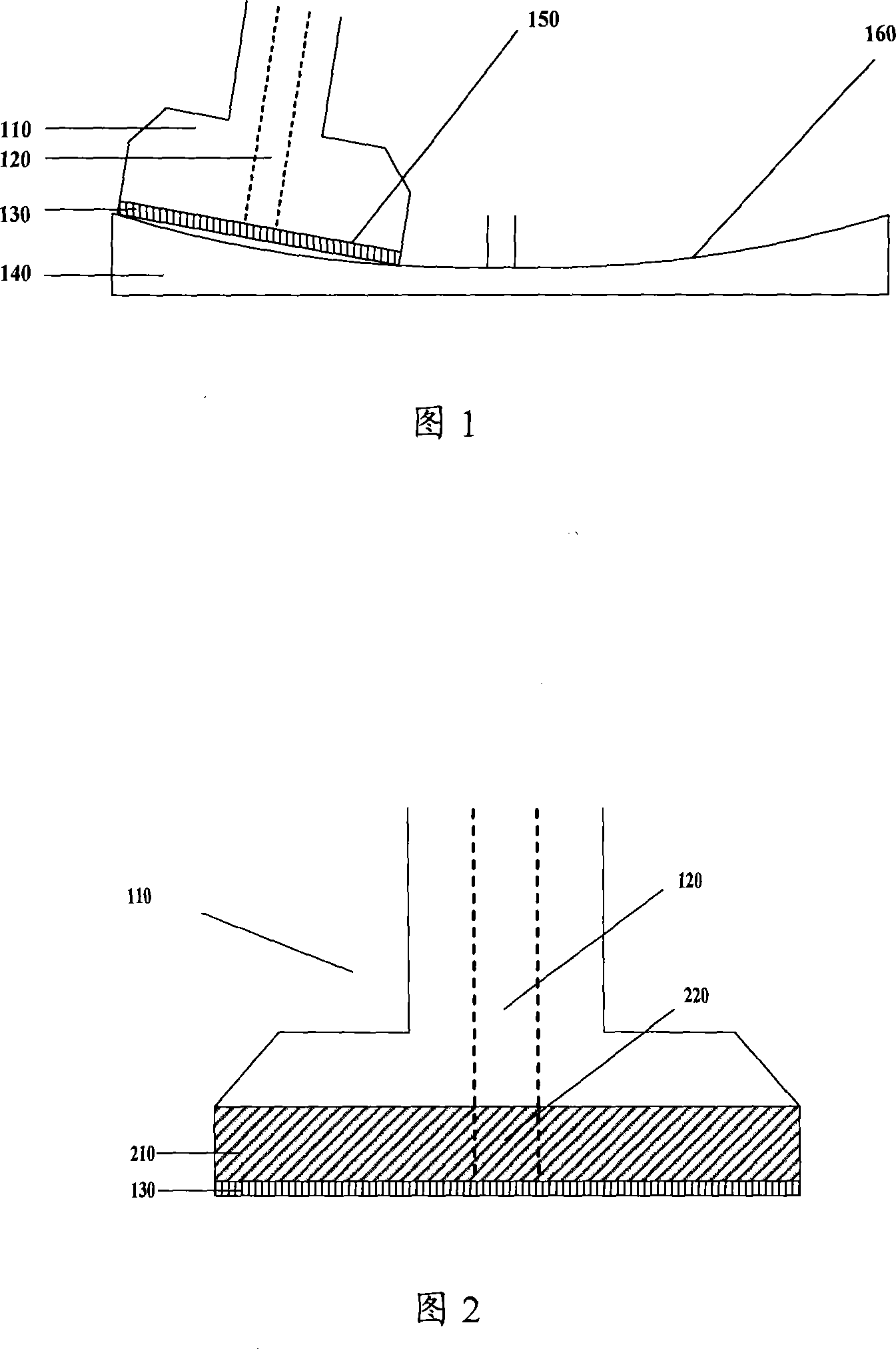
[0029] Fig. 1 is a schematic structural diagram of a grinding head and a grinding disc during the angle grinding process of a silicon wafer edge angle grinding device according to an embodiment of the present invention. As shown in FIG. 1 , the silicon wafer edge grinding device of th...
PUM
 Abstract
Description
Claims
Application Information