An electrostatic protection structure of high voltage drive integrated circuit

An integrated circuit, high-voltage drive technology, applied in the direction of circuits, circuit devices, emergency protection circuit devices, etc., can solve the problems of inability to effectively protect integrated circuits, flow, and drive the output pins of integrated circuits to burn out, so as to improve electrostatic discharge Protective ability, the effect of preventing electrostatic discharge

Inactive Publication Date: 2010-05-19
HOLTEK SEMICON
View PDF4 Cites 0 Cited by
  • Summary
  • Abstract
  • Description
  • Claims
  • Application Information

AI Technical Summary

Problems solved by technology

The method is to use a driver integrated circuit (Driver) of a metal oxide semiconductor field effect transistor (Metal OxideSemiconductor Field Effect Transistor, P-MOSFET) 11 with a larger output pin to connect to the input / output pin pad 12, and at the same time The metal oxide semiconductor field effect transistor 11 and the connection point of the input / output pin pad 12 are also connected with a resistor 13 as an electrostatic discharge protection circuit. The disadvantage is that the drive integrated circuit itself must have good electrostatic protection capability
In order to improve the electrostatic protection ability and heat dissipation effect of the driving integrated circuit, the volume of the driving integrated circuit must be increased to meet the aforementioned requirements. However, in electronic products that require light, thin, short, and small At the same time, it is not a simple matter to form a ring isolation (Ring Isolation) in the process of processing such a large-volume driver integrated circuit, and it is also prone to electrostatic discharge and large current parasitic in the bipolar In the path of the transistor (BJT), the output pin of the driver IC is burned
[0004] Another method is to add a diode (Diode) to the input / output port (I / O) of the output pin as an electrostatic discharge protection circuit, but when the actual ESD Vdd- (Vdd negative polarity mode) and Vss+ (Vss positive polarity mode) occur , the large current of the electrostatic discharge will not flow through the diode, and may flow into the integrated circuit and burn the internal circuit, thus failing to achieve the role of electrostatic discharge protection
[0005] Both of the above two known technologies cannot effectively protect the integrated circuit from the influence of electrostatic discharge. The present invention is just a circuit structure to solve this problem.

Method used


Image

  • An electrostatic protection structure of high voltage drive integrated circuit
  • An electrostatic protection structure of high voltage drive integrated circuit
  • An electrostatic protection structure of high voltage drive integrated circuit

Examples


Embodiment Construction

[0077] The detailed structure of the present invention and its connections are now described in conjunction with the following drawings to facilitate a further understanding of the present invention.

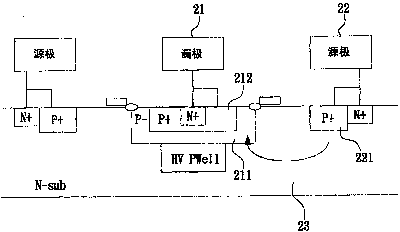
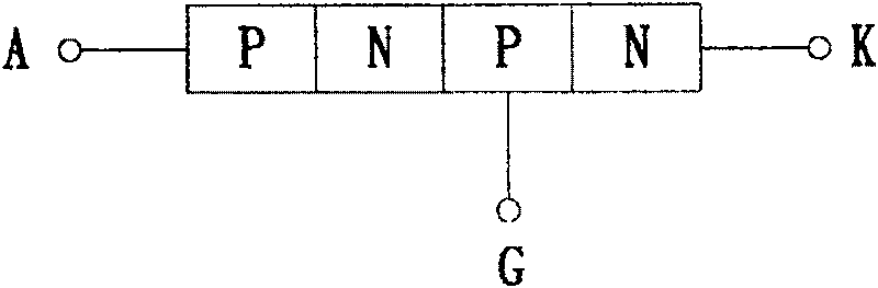
[0078] see Figure 2A , Figure 2A The structural diagram of the silicon-controlled rectifier added to the high-voltage drive integrated circuit of the present invention; wherein, the metal oxide semiconductor field effect transistor includes at least a drain (Drain) 21 and a source (Source) 22, and its output pin (source) Between the pole 22 and the drain 21) a silicon controlled rectifier (Silicon Controlled Rectifier, SCR) is added. Please also see Figure 2B As shown, wherein, the silicon controlled rectifier is an electronic component composed of a PNPN interface, passing through the P+ dielectric 221 of the source (Source) 22 to the N-type substrate 23, and then from the N-type substrate 23 to the drain (Drain) 21 P- dielectric 211 or P+ dielectric 212, and then forming...


PUM


Abstract

The invention relates to an electrostatic protection structure of a high-voltage drive integrated circuit, which includes: a current limiting element, which is used for limiting the amount of the current that flows to the high-voltage drive integrated circuit and is connected with an input / output pin port of the high-voltage drive integrated circuit; at least one electrostatic discharge protectiondevice, which is used for preventing the big current that is generated by electrostatic discharge from damaging the high-voltage drive integrated circuit and is connected with the input / output pin port of the high-voltage drive integrated circuit; a metal oxide semiconductor field effect transistor, which is attached with a silicon-controlled rectifier at the output pin; a power clamping circuit,which is used for limiting the amount of output current of a power end and is connected with a source and a drain end of the metal oxide semiconductor field effect transistor in series.

Description

technical field [0001] The invention relates to an electrostatic protection structure of a high-voltage driving integrated circuit. Background technique [0002] Generally speaking, no electrostatic discharge (Electrostatic Discharge, ESD) protection circuit is installed in the driving circuit of the known vacuum fluorescent display (Vacuum Fluorescent Display, VFD). An integrated circuit (IC) can hardly achieve any ESD protection effect by itself, so additional methods are needed to achieve the goal. [0003] see figure 1 , figure 1 Shown is the structural diagram of the electrostatic protection circuit of the known high-voltage drive integrated circuit. The method is to use a driver integrated circuit (Driver) of a metal oxide semiconductor field effect transistor (Metal OxideSemiconductor Field Effect Transistor, P-MOSFET) 11 with a larger output pin to connect to the input / output pin pad 12, and at the same time A resistor 13 is also connected to the connection point...

Claims


Application Information

Patent Timeline
Patent Type & Authority Patents(China)
IPC IPC(8): H02H9/00H01L23/60H01L27/00
CPCH01L2924/0002
Inventor 邓志辉吴钧晖张藤宝
Owner HOLTEK SEMICON
Why Eureka
Try Eureka