High-density antifuse semiconductor memory

An anti-fuse, semiconductor technology, applied in the direction of semiconductor devices, electrical solid devices, electrical components, etc., can solve the problems of unfavorable IC integration, low utilization rate of silicon wafers, etc., and achieve the effect of increasing density

Inactive Publication Date: 2011-09-07
UNIV OF ELECTRONICS SCI & TECH OF CHINA
View PDF2 Cites 0 Cited by
  • Summary
  • Abstract
  • Description
  • Claims
  • Application Information

AI Technical Summary

Problems solved by technology

[0006] The disadvantage of the existing technology is that the utilization rate of silicon chips is not high, which is not conducive to the integration of IC

Method used


Image

  • High-density antifuse semiconductor memory
  • High-density antifuse semiconductor memory
  • High-density antifuse semiconductor memory

Examples


Embodiment Construction

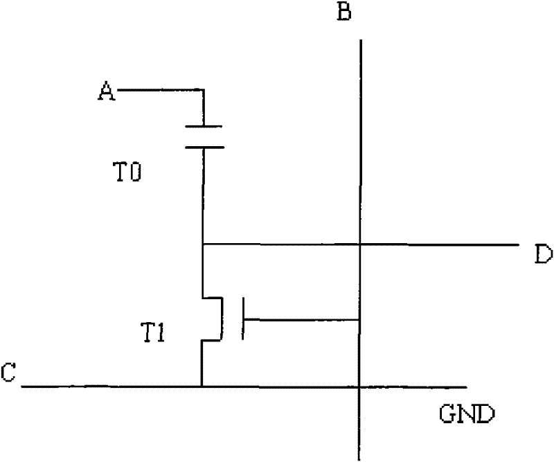
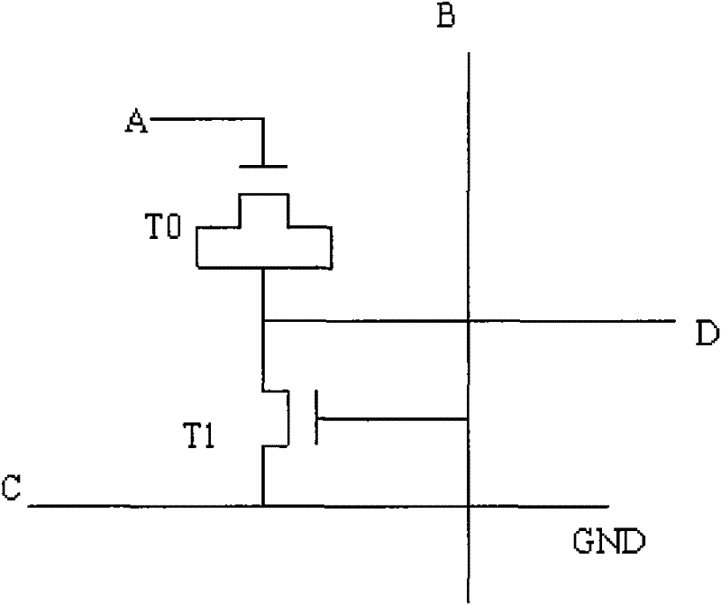
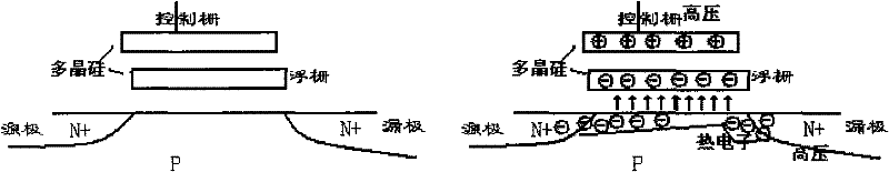
[0017] EEPROM / Flah (electrically erasable memory / flash memory) adopts a double-layer gate (two-layer poly) structure, the main structure is as follows image 3 shown. The basic principle is that when there is no electron injection in the floating gate, when the voltage is applied to the control gate, the electrons in the floating gate go to the upper layer, and holes appear in the lower layer. Due to the induction, electrons are attracted and the channel opens. If there is electron injection in the floating gate, that is, the threshold voltage of the tube is increased, the channel is in the closed state, storing logic '0', if there is no electron injection in the floating gate, the channel is in the open state, storing logic '1' '. In this way, the data storage function is realized.

[0018] In the EEPROM / Flash process, a double-layer gate (two-layer poly) process is adopted, that is, image 3 As shown in the control gate and floating gate, the present invention utilizes t...


PUM


Abstract

The invention discloses a high-density antifuse semiconductor memory, relating to an integrated circuit, in particular to a semiconductor memory and a programmable logic device. The invention comprises a plurality of memory cells, and each memory cell is composed of an MOS tube and a memory capacitor. The invention is characterized in that parts of or all memory capacitors form a plurality of capacitor groups; each capacitor group is composed of three or more memory capacitors sharing one polar plate. The invention fully utilizes the limited area of a silicon chip and improves the density of a non-volatile disposable programmable semiconductor memory.

Description

technical field [0001] The present invention relates to integrated circuits, in particular to semiconductor memories and programmable logic devices. Background technique [0002] Non-volatile programmable semiconductor memory is widely used in the field of electronic technology. Non-volatile means that the memory can still save data after power failure, and one-time programmable means that the memory can be written once by the user after leaving the factory. , then the data cannot be modified. [0003] The U.S. Patent No. 6215140 discloses the principle of storing data by using the silicon dioxide dielectric breakdown between the two plates of the capacitor. In this invention, a capacitor and a diode are connected in series at the intersection of the word line and the bit line. After the silicon dioxide dielectric between the two plates of the capacitor is broken down, there is a current path between the word line and the bit line. At the intersection point of , there is n...

Claims


Application Information

Patent Timeline
Patent Type & Authority Patents(China)
IPC IPC(8): H01L27/115H01L29/41
Inventor 李平李威谢小东李文昌
Owner UNIV OF ELECTRONICS SCI & TECH OF CHINA
Why Eureka
Try Eureka